
|
|
|
Instructor
Prof. Bevan Baas
| Mon | Tue | Wed | Thur | Fri | |
| Madan Shivakumar mshivakumar@ucdavis.edu |
2:15pm–3:15pm |
1:10pm–4:00pm Lab A01 4:10pm–7:00pm Lab A02 |
|||
| Bevan Baas |
4:30pm–open |
4:30pm–open |
12:30pm–1:30pm |
Lecture
TTh, 3:10pm–4:30pm
Physics 130
Textbook
 Digital Integrated Circuits, A Design Perspective
by Rabaey, Chandrakasan, and Nikolic
2nd edition, ISBN-13: 9780130909961
All work must be submitted at one time rather than in parts.
If the assignment is reviewed in class or solutions are made available, no credit is possible for late work. If the assignment was not reviewed in class, work may be submitted with a 1/3 reduction of remaining credit (i.e., 100% → 67% → 44% → 30% ...) per day. Unreviewed late work may be submitted with a verifiable written excuse.
Each homework sub-problem will be graded on a three-step scale: 0 (not a full effort), 1 (close but fundamental problem), and 2 (correct or with a very minor problem). For more challenging problems or those with many points, points may be multiplied, e.g., [0,2,4 pts] or [0,3,6 pts]; or graded on a similar five-step scale: 0% (not a full effort), 25% (between 0%-50%), 50% (close but fundamental problem), 75% (between 50%-100%), 100% (correct or with a very minor problem).
The Final project will be done individually and consists of the complete design of a CMOS chip including datapath, control, I/O, power distribution, clock distribution, and pad circuits.
The final exam is a mandatory component of this course. Unfortunately, no early or late exam is possible.
Quizzes and exam(s) cover all material from assigned readings, lectures (including posted notes), homework, and projects. Some exam material may be present in only one of these sources.
Bring pencils, eraser, calculator (sorry, no phones), colored pencils or pens, and one page of hand-written notes (both sides ok). No need to include specific device, material, or process data such as capacitance/area or resistivity; they will be provided to you on the exam if needed.
Non-obvious or very minor grading issues will not be considered—due to fairness to all students, the inherent subjectiveness of grading which is rife with both missing-points and additional-points imperfections, and because it is physically impossible to go through submitted work of every student in minute detail (which would be required for perfect fairness). To request a regrade, submit the following to the instructor: 1) a short description of the suspected grading error, 2) the following statement on your regrade request with your signature immediately below it: "I certify that I have not altered this work in any way after it was returned to me. I understand that such altering would constitute a violation of the Code of Academic Conduct." Note that to discourage falsified regrading, some number of all graded quizzes/exams will be photocopied before being returned.
Notify the instructor of clear and significant grading errors within a week of being returned. Due to the inherent subjectiveness of grading and to be fair to all students, only truly significant mis-grades will result in a grade change. Submit to the instructor: 1) a short description of the suspected grading error, 2) the following statement on your regrade request with your signature immediately below it: "I certify that I have not altered this work in any way after it was returned to me. I understand that such altering would constitute a violation of the Code of Academic Conduct." Note that to discourage falsified regrading, some number of all graded assignments/labs/exams will be photocopied after the initial grading.
Unfortunately it is generally impossible to make exceptions to the normal flow of the course (e.g., deadlines, rescheduling exams, etc.) other than for highly unusual circumstances (e.g., a medical emergency), in which case you must submit a written verifiable excuse to the instructor.
Unless stated otherwise, all work must be done individually—meaning done entirely by the student whose name is on the work. At the same time, discussing appropriate high-level concepts with other students are important steps in the learning process and are strongly encouraged.
The course Collaboration Policy explains the fine line between working together appropriately and inappropriately..
All future items are tentative. Changes are normally colored in green font.
| Date | Reading | Lecture | Notes & Slides | Assignments | Lab |
| Th, September 28 | - | Course and VLSI introduction, VLSI fabrication technologies |
• Lecture 1 slides • Slides 73-76  |
- |
Lab week 0: No lab |
| Tue, October 3 |
Ch. 1 |
Intro II, Design styles |
• Introduction II • Basic Units • 7 Basic diagrams • Basics of technologies • Chip implement methods |
Read "Cramming more components
onto integrated circuits," Gordon Moore, Electronics,
April 19, 1965.
This is the landmark paper which defined "Moore's Law."
If you are unfamiliar with static CMOS gates, see the textbook pages 180, 239, 241 for the inverter, NAND, NOR. |
Lab week 1: Setup environment and magic beforehand. Tutorials 1, 2, 3 |
| Th, October 5 |
Ch. 2 |
Abstraction of complexity, Cost, yield |
• VLSI is like art • Abstractions of complexity • VLSI costs |
Hwk 1, problems 1 and 4 only.
For problem 4, use the IEEE website to find papers from the 2023 International Solid-State Circuits Conference (ISSCC) which is widely considered the top chip conference in the world for advanced chips. Accessing the web site is free from campus or a UCD VPN. Find the table of contents by searching for: "ISSCC 2023 Table of Contents". See the Course Glossary when helpful. Some data may not be listed in papers. Tabulate chip data for all papers in Sessions: 2 (Digital processors), 9 (Highlighted chip releases: digital and machine learning procs), 17 (High-speed data converters), and 33 (Non-volatile memory and compute-in-memory), by searching for: "2023 IEEE International Solid-State Circuits Conference" session x (with quotes) which will then return paper titles from that session. Find the actual papers (which are 1-page plus figures) by searching for the title. Note: "device" = "transistor". When available, normally click on the small red pdf icons, not links. 2:45pm: Upload to canvas. |
|
| Tue, October 10 | - | Ch 2: CMOS Fab I |
• Fab materials & processes |
- |
Lab week 2: Tutorials 4, 5, 6 |
| Th, October 12 |
Ch 3: pp. 116-117 (latchup). |
CMOS Fab II, Full-custom layout, Design rules, Stick diagrams, Magic abstractions vs. GDSII, |
• Photomasks • Three fab examples • Advanced metal interconnect examples • Full-custom layout & magic • Design rules |
- | |
| Tue, October 17 |
Ch 5.1-5.3.2 Ch 5.4-5.4.2 |
Layout guidelines, |
• Multi‑project wafer organizations – MOSIS, LA – Muse Semi [notes], SanJose – CMP, France • Stick diagrams • Magic vs. GDSII/CIF • Layout Guidelines (hand drawn) |
"Morris Chang: Foundry Father (TSMC)," T. Perry, IEEE Spectrum, April 2011. |
Lab week 3: Tutorials 8 and 11 (Sec. 4 only) |
| Th, October 19 |
Ch 3: pp. 104-113. Sec 4.3.2: pp. 144-146 [resistance] |
Layout guidelines II, |
Hwk 2, due Th, Oct 19, 2:45pm "How the Father of FinFETs Helped Save Moore's Law," T. Perry, IEEE Spectrum, April 2020. |
||
| Tue, October 24 |
Layout guidelines III, Nwell, pwell, and their contacts Latchup, Ch 5: CMOS inverter characteristics I |
• VLSI In The News: Undersea datacenter |
Lab week 4: Simulating layout. Work through Irsim Tutorial. |
||
| Th, October 26 |
Quiz 1 Ch 5: CMOS inverter characteristics II robustness; |
||||
| Tue, October 31 |
Ch 3: Sec. 3.5 [scaling] |
Fanout, fanin; FO4 Inverter performance Ch 3: MOS resistance |
• Notes-ch3 | Read "The Fanout-of-4 Inverter Delay Metric," David Harris, et al., unpublished, ˜1997 which introduces the concept of the "FO4" delay metric. |
Hwk 3, due Wed Nov 1, end of lab Lab week 5: Irsim simulator |
| Th, November 2 |
Ch 7: pp. 326-334, 344-346,
358-360, 368-372 [seq. circuits] |
MOS capacitances Sheet resistance, Ch 3: Scaling, Ch 7: Sequential circuits, clocking, |
|
"A Better Way to Measure Progress in Semiconductors," S. Moore, IEEE Spectrum, August 2020. [pdf] | |
| Tue, November 7 |
Ch 5.4.3 [overall perf.] |
Ch 7 II:
ring oscs, latches and flip-flops |
• Flip-flop schematics | "Design of Ion-Implanted MOSFET's with Very Small Physical Dimensions," Robert H. Dennard, et al., IEEE Journal of Solid-State Circuits, October 1974. This is the landmark paper which defined "Dennard Scaling." Read pages 257, 258, and "Cir. Perf. with Scaled..." section on pages 264–266. Skim the rest. He uses κ for what we call S. |
Lab week 6: Flip-flops |
| Th, November 9 |
CMOS inverters: sizing for performance |
||||
| Tue, November 14 |
Ch 6: pp. 236-251, 269-271 [comb. CMOS] Ch 6: pp. 277-280 (pass-trans) |
Sizing for performance II, Chain of inverters design, |
• VLSI
In The News: World's Largest Chip • Chain of inverters |
Hwk 4, due Wed Nov 15, end of lab Lab week 7: Flip-flop cells |
|
| Th, November 16 |
Ch 4 (Wires) |
Quiz 2 Ch 6: Combinational CMOS logic gates static, |
|||
| Tue, November 21 |
Ch 9: pp. 445-462 (pads, grids,...). |
ratioed, dynamic, pass-tranistor
|
• VLSI
In The News: Nano Sheets |
"The Nanosheet Transistor is the Next (and Maybe Last) Step in Moore's Law," P. Ye, IEEE Spectrum, July 2019. |
Lab week 8: More complex cells |
| Th, November 23 | Happy Thanksgiving

|
||||
| Tue, November 28 |
Sec. 9.3.2: pp. 462-464 (electromigration). Ch 12: pp. 623-634, 657-662, skim 663-669, 672-674 (memories). |
Transmission-gates
Wires |
• VLSI In The News: Samsung $17B plant in Austin, TX • Wires • OnChipInductors |
"Big Trouble in Little Interconnects," S. Moore, IEEE Spectrum, January 2023. |
Lab week 9: Adders Hwk 5, due Wed Nov 29, end of lab |
| Th, November 30 |
Ch 8: pp. 377-388, 396-406,
423 (implementations). Ch H: pp. 721-737 (test). |
Std cell P&R chip design Chip-level structures and issues I, |
• VLSI
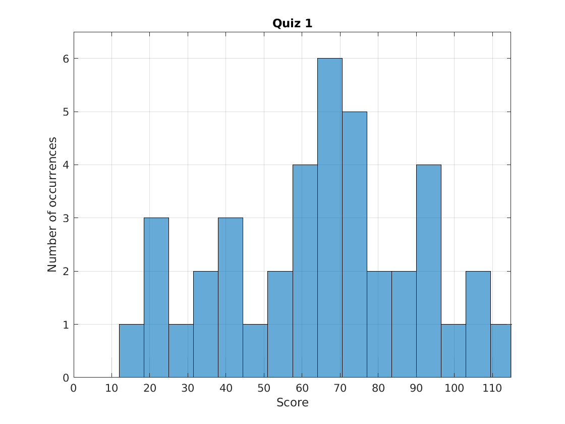
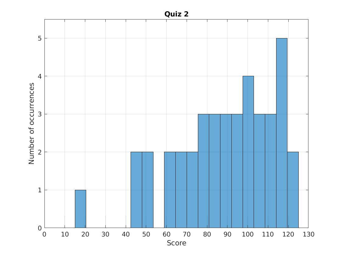
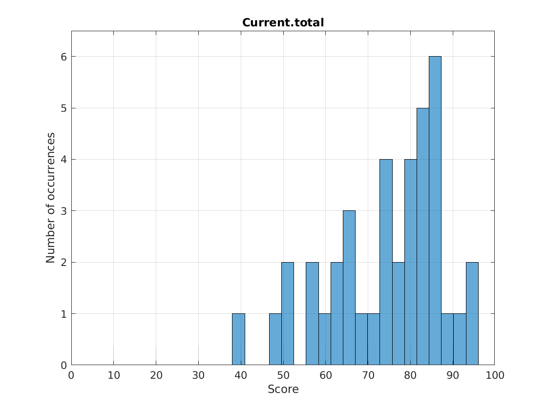
In The News: Backside power in TSMC's 2nm node • Graphene wires • Std cell design • Histogram: quiz 1 • Histogram: quiz 2 • Histogram: current total |
"Next-Gen Chips Will Be Powered From Below," B. Cline, IEEE Spectrum, August 2021. | |
| Tue, December 5 |
Chip-level structures and issues II |
• VLSI
In The News: Chip shortage and Qualcomm |
Lab week 10: Chip-level structures Hwk 6, due Wed Dec 6, end of lab |
||
| Th, December 7 |
FIB edits, Spare gates, Packaging, Ref: Memories, Ref: Multipliers, |
• Electromigration (chip issue) • FIB editing • Spare gates • Packaging • Datasheet 132-pin PGA • Ref:Memories • Ref:Multipliers |
"Single-Chip Processors Have Reached Their Limits (Chiplets)," M. Smith, IEEE Spectrum, April 2022. | ||
|
Office hour: Fri Dec 8 12:30-1:30, Prof. Baas, Kemper 2037 Office hour: Sat Dec 9 1-2pm, Madan, Kemper 2107 Office hour: Mon Dec 11 1-2pm, Prof. Baas, Kemper 2107 Office hour: Tue Dec 12 2-3pm, Madan, Kemper 2107 |
|||||
| Wed, December 13, 8:00am–10:00am |
Final exam (notes) |
||||
| Th, December 14 10:00 am: Deadline to upload files to canvas 10:00 am–6:30 pm Functional demonstration to TA in 2107, last chance Sign up ONLY ONCE: Reservation spreadsheet. |
Final project | ||||
A wide variety of die photos at: http://diephotos.blogspot.com/, most of which appear to be older-generation full-custom designs.
