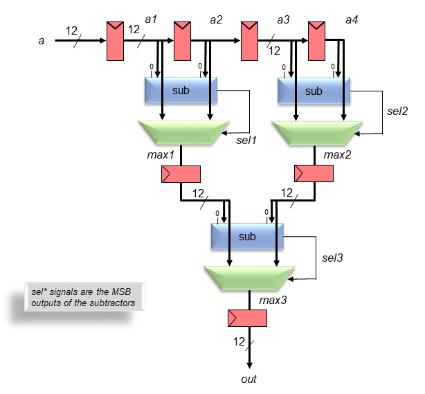
Figure 1. Top-level block diagram
This project consists of the design and layout of a chip which finds the maximum value among the last four 12-bit numbers to enter the chip. It is a type of sliding window filter often used in digital signal processing workloads.
All work must be done individually.
input a = {ab, aa, a9, a8,...a2, a1, a0} (12 bits)
Values of a are non-negative ranging from 000000000000 (zero) to 111111111111 (4095 base10).
input clk (clock signal)
output out = {outb, outa, out9, out8,...out2, out1, out0} (12 bits)
The value of out has the same range as the input a.
As explained in class, the maximum of two numbers is found by subtracting using the following method. For example x – y:
  x      00000 0000 0110   (+6, spaces added for readability only)
  y    - 00000 0000 0001   (+1, spaces added for readability only)
      ------------------
         00000 0000 0101   (+5 difference)

  x      00000 0000 0011   (+3, spaces added for readability only)
  y    - 00000 0000 0100   (+4, spaces added for readability only)
      ------------------
         11111 1111 1111   (-1 difference)
In this example, if the difference is positive, x is larger, if the
difference is negative, y is larger. If zero, obviously either x or y can
be chosen as the larger value.
A 2's complement number is positive or zero if the MSB (red font above) is zero. It is negative if the MSB is one.
Before subtracting the 12-bit unsigned numbers, it is necessary to first convert them into 13-bit 2's complement values that can be subtracted. This is done by appending a zero in the 13th-bit MSB position (see green zero below).
   xxxx xxxx xxxx   (12-bit unsigned value)
  0xxxx xxxx xxxx   (13-bit signed 2's complement value)
Build a 12-bit subtractor by building a 13-bit ripple-carry adder for the two 13-bit 2's complement inputs.
Calculate x – y by instead calculating x + (–y) which is found by connecting x to one input of the adder, and the inverted bits of y to the other adder input, and connecting 1 = Vdd to the carry_in of the LSB of the adder. (Recall that numbers are inverted in 2's complement by "flipping the bits and adding one".)
Although the three max* signals can be 12 or 13 bits, recall their MSB bits are always zero, so to save circuits, make all muxes and max* signals 12 bits wide.
Design a clock driver chain of inverters which is located in one location (not spread around the chip) beginning with a 12 λ/6 λ inverter (driven by the clock input pad) and which drives the clock wire network without an inversion from the clock signal, and which has fanouts of internal buffers no larger than 6. Estimate wire capacitances of the network using these wire capacitances, Assume a 12 λ/6 λ inverter has an input gate cap of 8 fF.
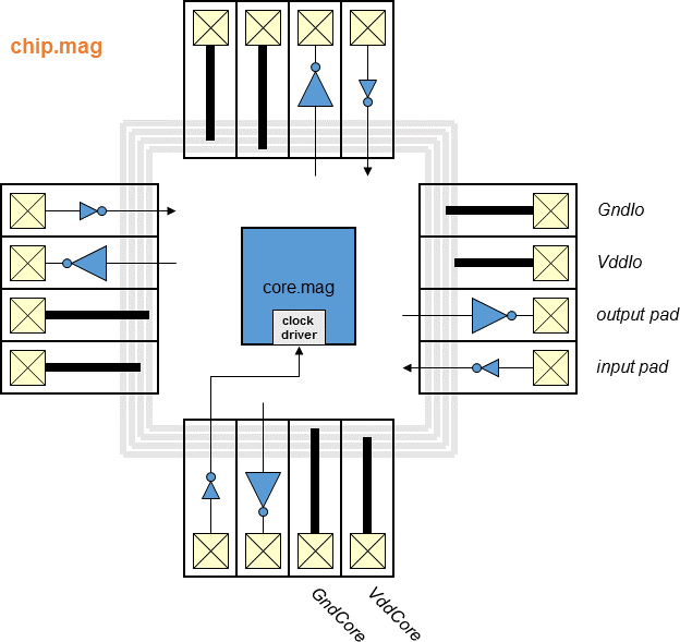
Place the entire clock distribution tree (wires) inside core.mag
Place the clock driver inside core.mag
The example simplified diagram below shows the hierarchy of the core, clock driver, power rings, and I/O pads.
Attach a label to each input signal and output signal using exactly the same signal name used in core.mag. It is probably not worth the effort to simulate chip.mag and instead better to simulate top.mag. In case you choose to simulate chip.mag, short VddCore and VddIo together and also GNDCore and GNDIo together and label them Vdd and GND respectively.
Power and Ground
a) Core power/ground: three VddCore and three GndCore pads for internal circuit power
b) I/O power/ground: include one VddIo and one GndIo for every four chip output pads, and one of each for every six chip input pads. The chip's input and output buffers are powered with VddIo and GndIo.
Input into chip: include at least two inverters (buffers) in each cell
Output out of chip: include sufficient buffering to drive the output pad with a fanout no larger than 8 at any point in the inverter chain. The NMOS and PMOS of the final inverter must be separated by at least 100 λ, and must be almost entirely surrounded by appropriate-type guard rings.
Assume pad and load capacitance is 9 pF. Copy the cell ninepF.mag to your directory and attach it to every output pad in a top level test cell (called top.mag), not in the same cell as your chip. It's large, but will make irsim timing simulations much more accurate.
Pad requirements:
place the pads in a single ring around the periphery of the chip
58 µm × 58 µm pad composed of all 6 metal layers
48 µm × 48 µm bonding area (paint glass in magic)
75 µm pitch (center-to-center distance)
consist of a stack of all metal layers
have all inter-layer vias on the periphery of the pad, not under the passivation opening
have no circuits under the pad
place I/O pad circuits in a reasonably small space 30 µm from the pad and 10 µm from the nearest power ring
Power rings. Design four power rings as part of each pad cell: VddIo, GndIo, VddCore, and GndCore. Each ring must be 30 µm wide and made of at least four levels of metal. Place the rings as close to the periphery of the chip as reasonable to maximize the internal circuit area.
Power grid. Route wide VddCore and GndCore wires (major ones at least 10 µm wide) across the entire chip connecting to the appropriate power ring on opposite sides and to your active circuits in the middle. You are required to build the power grid only in the regions that supply your circuits.The example diagram below shows the hierarchy of the chip and the test environment in top.mag
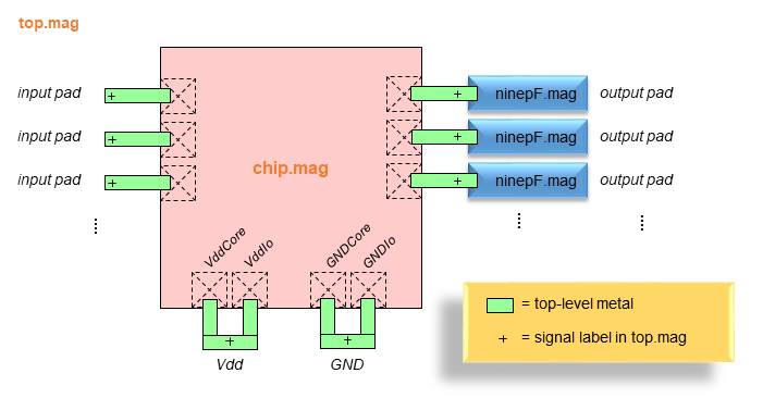
Attach a large piece of top-level metal to each input and output pad of your chip. Short VddCore and VddIo together and also GNDCore and GNDIo together using top-level metal. Attach a label to each piece of metal using exactly the same signal name used in chip.mag.
Attach a ninepF.mag load to each chip output.
Follow the Special Nanometer-scale rules for EEC 116 for all layout including pad circuits.
Use only static circuits except where explicitly permitted or required. Transmission-gate logic may be used for only the following circuits: XOR, XNOR, full adders, muxes. If you use transmission-gate logic, be careful for possible issues mentioned in class when signals and their inverted versions change at different times and can cause simulations to go "X" if inverters are not placed to prevent signals fighting.
Flip-flops. All flip-flops must be clocked on positive clock edges. Use the "safest" flip-flop design from the handout. Include two inverters as clock buffers inside each flip-flop cell as explained in lecture (omitting them risks running into serious simulation problems).
All transistors must be minimum length unless specified otherwise.
Make all Vdd and Gnd wires (e.g. the main power wires in cells) at least 8 λ wide.
Internal signals may be inverted or not inverted from what is shown in the main diagram, however the operation and internal logic must be as described.
Do not optimize circuits (dynamic, ratioed, etc.), architectures (pipelining, iterative datapaths, faster arithmetic algorithms, etc.), or other aspects beyond VLSI design techniques.
The tbtest.cmd (version 1.4, 2023/12/13 16:45) and 1clk.cmd .cmd files will be used during the grading of your design using fresh versions. Download and modify mysetup.cmd to set the stepsize (clock frequency) and analyzer signals. You will likely find it helpful to add tests when tracking down bugs.
Make an irsim waveform with every input and output signal name and print it out so that all data values are visible in hexadecimal or base10.
While the final tests will be performed in only the top.mag test environment (see above), it is a good idea to use the same I/O labels for both core.mag and top.mag (and chip.mag if you choose/need to run tests at that level also) so identical or almost-identical cmd files tests may be used for all testing scenarios.
Simulate your chip with correct outputs using a very long stepsize (for example, "stepsize 100")
Iterate until the difference in stepsize between simulations with and without "pending events" messages is 0.01 (nsec).
                  _____       _____
   clock    _____|     |_____|
   during
   test          |     |     |
              -->|     |     |<-- irsim simulation cycle time
              -->|     |<-- stepsize (minimum cycle time when no pending events)
                  __    __    __
   clock    _____|  |__|  |__|  |__
   at max
   frequency
For example, if the shortest stepsize without pending events is
0.9 ns, the irsim simulation has a clock cycle time of 1.8 ns
(560 MHz).
However the circuit can run at a maximum frequency of 1/0.9 ns =
1.1 GHz.
Total: 420 points = 270 pts + 150 maximum performance pts
b) [10 pts] Output pad driver: calculations, transistor schematic with widths
c) [10 pts] Floorplan drawing showing the location of each block in core.mag
d) [20 pts] Complete magic layout of core.mag demonstrated to TA and all *.mag files uploaded.
e) [20 pts] Complete magic layout of chip.mag demonstrated to TA and all *.mag files uploaded.
f) [125 pts] core.mag, test sequence(s) listed above. Demonstrate to your TA.
g) [50 pts] top.mag, test sequence(s) listed above. Demonstrate to your TA.
h) [25 pts†] Measured maximum clock rate of top.mag Demonstrate to your TA.
i) Performance points. Area, Delay (max logic delay), and A × D are critical parameters in VLSI design. Since we do not know ahead of time how small the circuit can be, grading will necessarily be calculated proportionately and relative to results of other groups in the class. For example, the group with the largest core.mag Area will receive the minimum number of points for the Area category and the group with the smallest Area will receive the maximum. In highly unusual cases, if a group achieves a poor result but clearly made an unusually-strong effort, the instructor may increase their points beyond the formula's recommendation.
[25 pts – 13 pts†] lower Area (core.mag) compared to class
[25 pts – 13 pts†] lower Delay (top.mag) compared to class
[100 pts – 50 pts†] lower Area (core.mag) × Delay (top.mag) compared to class
† No (h) Max clock rate or (i) Performance points are possible for designs that:
Canvas submission: All *.mag files and NO *.ext, *.sim, or *.cmd files (except mysetup.cmd with your shortest achievable stepsize), must be uploaded in a single .zip file by the posted deadline.
If you care about your grade, perform a "practice run" on your .zip file in an empty directory after creating it, using fresh copies of tbtest.cmd and 1clk.cmd, to make sure your layout is complete and all simulations work at your minimum stepsize during your checkoff meeting.
Paper submission: Fill out and submit 1) this Key Results Summary Sheet, and 2) other requested printed material, to your TA during your checkoff meeting.
Shortly after the posted deadline, all .zip files will be downloaded from canvas (late submissions will not be tested).
Checkoff meeting: Meet with your TA at your reserved time. The following steps will be followed for each student during the checkoff.
mkdir student_name
mv download.zip student_name/
cd student_name/
unzip download.zip
rm *.ext *.sim tbtest.cmd 1clk.cmd
less mysetup.cmd (give it a quick look)
cp ../tbtest.cmd ../1clk.cmd ./
magic116 top.mag (layout examined, extracted)
ext2sim116 top
irsim116 top.sim
@ tbtest.cmd
Be logged into a workstation in case there are any very simple issues that might come up however there is no time for debugging.
The most important recommendation is to focus entirely on getting your design functional before doing any optimizations. A very large proportion of the points can be earned only with a fully working design. The reason for this is because it is possible to get many things working while stil having many serious bugs, and the only way to know the measurements are reliable is if the layout simulates correctly.
The second most important recommendation is to believe that achieving a working design takes more (perhaps much more) time than you expect. Based on past experience, students that do not finish their project typically a) start two days before the deadline, or b) spend too much time optimizing small blocks and underestimate the time required to connect blocks, complete chip-level structures, and debug their design.
The project definitely is do-able in the given time especially considering you should already have several working key components such as flip-flops and others. There are an infinite number of ways to design the project correctly and an infinite number of ways to design the project incorrectly and while we have gone over all necessary background material during the quarter, it will certainly require some hard thought and very careful design and debugging effort to create a correct design. I strongly encourage you to read and apply posted Tips here and elsewhere.
Tips for Debugging and Speeding Up Circuits using Magic and IRSIM
Reference matlab files
testgen.m may be useful
test.cmd.example example output file
2023/12/02  Posted
2023/12/04  Corrected the process of converting unsigned to 2's complement--it
            is done by appending a zero bit.
            Removed negative inputs from Functional Testing section.