Mon | Tue | Wed | Thur | Fri | |
Kevin Gubbi kgubbi@ucdavis.edu |
5:00pm–6:00pm (zoom) |
4:10pm–6:00pm Lab Kemper 2107 |
||
Bevan Baas |
1:00pm– SocSci 70 |
A single grade is given for both 181A and 181B and is assigned at the end of 181B. At the end of 181A, a grade of "IP (In Progress)" is assigned and then later converted to the final grade.
Normally late work can not be accepted after its deadline however if a serious issue such as an illness prevents you from completing work on time, obtain a verifiable written excuse, bring it to the instructor, and something will be worked out.
In this course, unless specified otherwise, all work must be done "individually"—meaning done entirely by the student whose name is on the work.
Make sure you fully understand the course Collaboration Policy and talk to the instructor if you have any questions.
Normally lab will be held in Kemper 2107.
Due to the large amount of grading for TAs and the fast pace of material in lab, credit for late lab work is not possible or minimal.
Checkoffs: late checkoffs are normally not possible.
Lab reports: late reports can not be accepted
Canvas uploads: the entire lab's grade will be reduced by 10% if late up to one day and reduced to zero after that. Please verify your upload to avoid penalty.
Incorrect canvas submissions (e.g., not matching demo code or with extraneous files) must be corrected by the student and will be considered late
Normally the TA will not be able to debug students' circuits in detail so they are available for other students. If the TA agrees to assist you in debugging your circuit, show your TA your design materials such as block and timing diagrams first. Normally, TAs will focus on teaching debugging techniques rather than finding a particular bug in your design.
Take care of your FPGA board and camera. You must buy a new one if you lose or break yours. They can be purchased from Terasic (plus expensive shipping) or perhaps other sources online.
Installing
Quartus, Modelsim, and SystemBuilder
The Quartus Prime Standard Edition is needed for the DE1-SoC board.
Notes on active high/low inputs/outputs for the DE-10 Lite and DE1-SoC
Displaying to a VGA monitor
Creating verilog-ready bitmaps from image files
Using the accelerometer on the DE10-LITE board (different for the DE1-Soc)
Misc: http://www.asic-world.com/ (some examples, however do not use if they conflict with class guidelines)
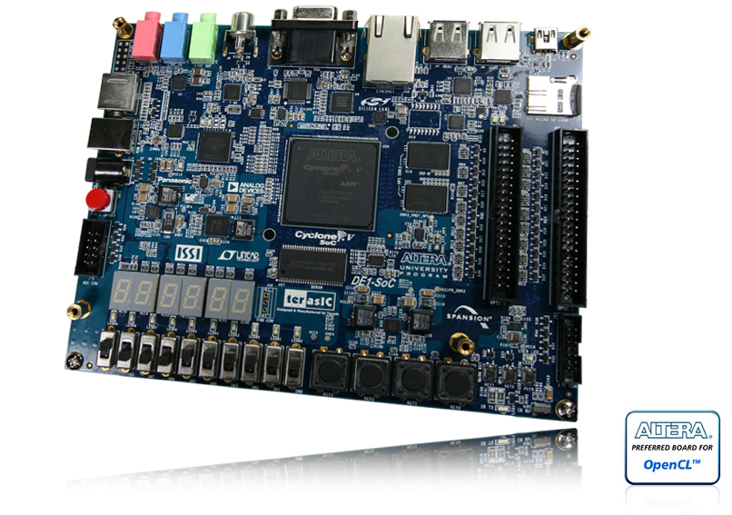
The Terasic DE1-SoC FPGA board
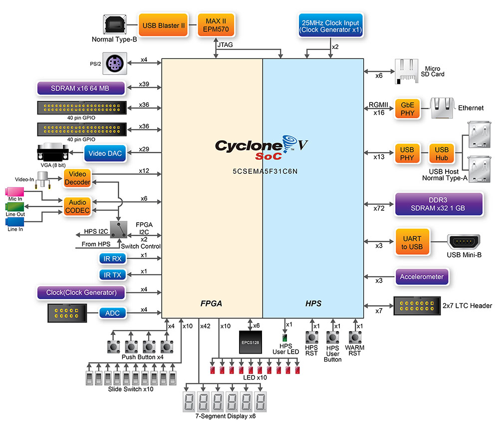
In lab you will use a Terasic DE1-SoC board which contains a Cyclone V SoC 5CSEMA5F31C6 chip.
The Cyclone V Device Handbook (best source of details for structures such as the DSP blocks)
Many of the early lectures will consist of a high-speed review of concepts covered in EEC 180 so your benefit will be far greater if you read the posted handouts before lecture and come with questions.
Future details are tentative.
Date | Lecture | Notes, Handouts, and Reading | Assignments |
Tue, Jan 9 |
Course introduction Digital design overview Basics of digital systems |
Lecture 1 notes |
|
Tue, Jan 16 | Verilog overview I |
Basic units Basic diagramsJAN 16 (minor notes regarding the pipelined block diagram) HDL to hardware Verilog 1: Overview Verilog 2: Basics |
|
Tue, Jan 23 |
Verilog overview II Binary number formats Binary coded decimal (BCD) Binary fractional Addition hardware Subtraction hardware Sign extension for 2's complement Memories Single-bit memory elements Flip-flops and 9 rules of using them Flip-flops with reset, preset, enable Four structures in HW verilog |
Lecture 3 notes Verilog quick ref guide, S. Sutherland (skim quickly) [orig] Verilog 3: Time and delay Verilog 4: Common mistakes Verilog 5: Testing Verilog 6: Decoder example Binary number formats Ref: Addition/subtraction Sign extension Single-bit memories (FFs) |
Lab 1 due Th, Jan 25 |
Tue, Jan 30 |
Memories I |
Four verilog constructs Memories |
|
Tue, Feb 6 |
Memories II M10K memory blocks Control circuits Counters Finite state machines |
M10K memories Control Circuits and Counters Finite State Machines |
Lab 2 due Th, Feb 8, 6:00pm |
Tue, Feb 13 |
Critical timing requirements of digital systems Pipelines Pipeline throughput and latency I |
Critical timing requirements Pipelining |
|
Tue, Feb 20 |
Clocks Multiple-frequency clocking Saturation I |
Clocks Variable-freq clock hardware Saturation |
Lab 3 due Tue, Feb 20 |
Tue, Feb 27 |
Saturation II VGA video interfaces VGA sync signals Pipeline throughput and latency II Pipelining systems |
– |
|
Tue, Mar 5 |
System-Level design Interfacing with unsync inputs: debouncing, edge detection Block interfaces, timing, interconnect Lab 5 video pixel processing overview |
Steps to design systems Interfacing input signals |
Lab 4 vga_top.zip due Tue, Mar 5 |
Tue, Mar 12 | Design consulting |
Design consulting |
Lab 5 DE1_D8M.v5.zip due Th, Mar 14 |
Date | Lecture | Notes, Handouts, and Reading | Assignments |
|
|||
Wed, Mar TBD | Course overview |
Lecture 11 notes |
|
Wed, Apr TBD | Group meetings |
Lecture 12 |
|
Wed, Apr TBD | Group meetings, Milestone #1 checkoff |
Lecture 13 |
|
Wed, Apr TBD | Group meetings |
Lecture 14 |
|
Wed, Apr TBD | Group meetings |
Lecture 15 |
|
Wed, May TBD | Group meetings, Milestone #2 checkoff |
Lecture 16 |
|
Wed, May TBD | Group meetings |
Lecture 17 |
|
Wed, May TBD | Group meetings |
Lecture 18 |
|
Wed, May TBD | Group meetings |
Lecture 19 |
|
Wed, Jun TBD | Group meetings |
Lecture 20 |
|
Jun TBD x:00-x:00pm Room TBD |
Group presentations • Group 1 • Group 2 • Group 3 • Group 4 • Group 5 |
|
Last update: March 21, 2024