This tutorial describes a simple method to drive a VGA monitor without requiring a large frame buffer memory. The provided VGA controller is configured for a resolution of 640 horizontal pixels × 480 vertical pixels because this is the supported resolution of the DE10-Lite board. With a 25 MHz pixel clock, the interface operates at approximately 59.5 frames per second.
On the DE10-Lite boards, the VGA interface uses 4 bits to represent each color. A value of 4'b0000 means the color is turned off. Thus, if all the red, green, and blue signals are set to 4'b0000, the screen will be black. A color value of 4'b1111 translates to full intensity. With all numbers inbetween representing a range of color intensities.
The signals available to you are "col" and "row" which indicate the horizontal and vertical pixel addresses respectively that the VGA controller is currently driving.
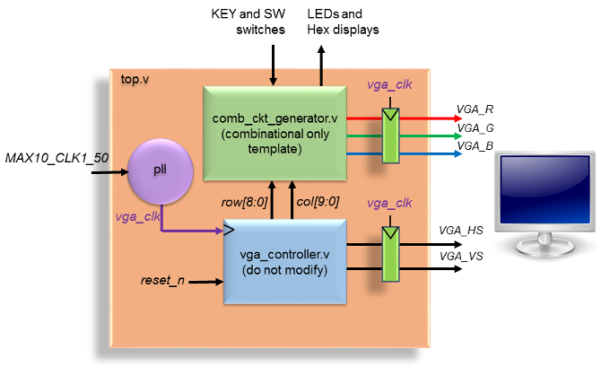
Figure 1. High-level block diagram of the VGA driver system. All code is provided including a comb_ckt_generator.v template file.
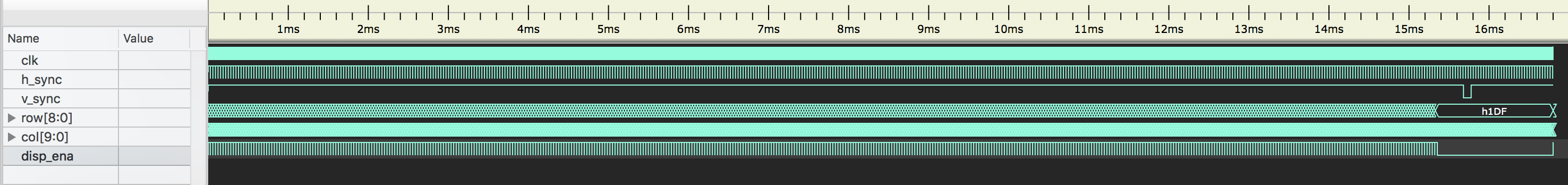
Figure 2. Key signals for a VGA display shown for an entire video frame.
The interface for a VGA video display is relatively minimal and simple. The signal v_sync (vertical sync) going low signals to the display that a complete picture frame has been drawn and to prepare for the next frame. This is shown in Fig. 2 on the far right side of the waveform plot.
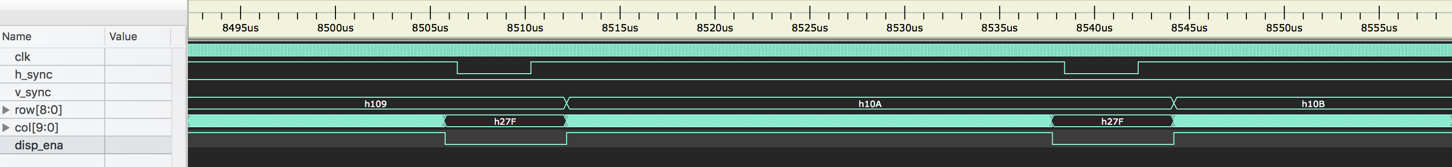
Figure 3. Key signals for a VGA display shown for an entire row of pixels and two partial rows.
Similarly, the signal h_sync (horizontal sync) signals to the display that a complete row of pixels has been drawn and to prepare for the next row. It can be seen pulsing low hundreds of times in Fig. 2 and also zoomed in for two low pulses in Fig. 3.
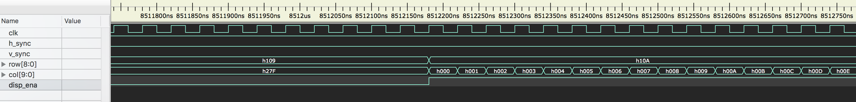
Figure 4. Key signals for a VGA display shown for the beginning of pixel row 266 (hexadecimal 10A = 9'h10A) where the column counter can be seen counting up from zero to decimal 14 = 10'h00E.
Figure 4 shows a set of waveforms from the same simulation showing pixel timing details. In this waveform, the clock is finally visible with v_sync and h_sync stable high, and row and col counting through horizontal pixels in pixel row 266. The red, green, and blue pixel colors are not shown in these waveforms.
A Quartus project with the necessary files to get started is posted below with the necessary code and PLL instantiations to interface with a 640 × 480 VGA display. The Quartus project should synthesize and run with no errors. If there are errors, please inform the professor or your TA.
A brief description of the main modules in the VGA project is given below.
-
pll.v, pll.qip, pll.ppf
To get correct timings, a Phase-Locked Loop (PLL) clock generator is needed to convert the 50 MHz clock on the DE-10 Lite to 25 MHz. This IP component handles the instantiation of the PLL.
pll.qip provides Quartus with generic information regarding the IP component such as the intended device, associated Verilog file and associated .ppf file. pll.v instantiates the PLL primitive and provides a module to connect input and output clocks. pll.ppf provides miscellaneous input and output pin data.
-
vga_controller.v
This module generates the necessary horizontal and vertical sync signals expected by the VGA receiver. In normal use, you should not need to use h_sync, v_sync, and disp_ena signals. Pixels are drawn one at a time from left to right and then top to bottom (see figure). Pixel (0,0) is in the upper left corner.
To help with drawing, vga_controller exports the following two signals:
-
row: The row (vertical coordinate) of the pixel being drawn.
-
column: The column (horizontal coordinate) of the pixel being drawn.
Note that the behavior of these signals is undefined when "disp_ena == 1'b0".
-
-
comb_ckt_generator.v
This is the combinational logic block that determines RGB color outputs given a certain row and column pixel and the position of the ten SW board switches.
-
top.v
This is the top level module in the design. It instantiate "vga_controller.v" and registers timing and color output signals.
Signals of interest include:
red, green, blue: 4 bit signals controlling the color that is to be drawn to the current "row" and "column" pixel on the display. A value of 4'b0000 means the color is not present while 4'b1111 means the whole intensity of the color is applied.
Using the provided code to draw is fairly simple. Given a "row" and "col" pixel coordinate (for 0 ≤ row ≤ 479 and 0 ≤ col ≤ 639 since we normally begin counting from zero in digital systems), you must create logic to assign the correct values of "red", "green" and "blue" to be drawn at the specific row and col coordinate in a single combinational logic block as indicated in block comb_ckt_generator.v in Figure 1.
Note that this is backwards from how drawing is performed using normal graphics hardware where a frame buffer is used to store an image before drawing. We use the previously-described method instead because the amount of memory required to implement a frame buffer is not readily available on the MAX10 FPGA.
To properly synchronize signals, all flip flops in your design must use the 25 MHz "vga_clk" clock signal and not the 50 MHz "MAX10_CLK1_50". The VGA interface indirectly uses a 25 MHz pixel clock.
It is often desirable to make certain updates only at the point in time after the drawing of one complete frame before the drawing of the next frame has begun—for example, in this way fast moving objects will not be drawn partially in one location and partially in another location.
The best way to do this is to synchronize the updating of critical values using the vertical sync signal (called "VGA_VS" in the provided code and shown in Figure 1). As detailed in the DE10-Lite_User_Manual.pdf manual, the interface contains specialized timing intervals including the vertical sync; fortunately these have been worked out for you in the provided code for normal operation.
The vertical sync signal pulses from high to low for many cycles and there are also many cycles both before and after the pulse which are not used for outputting pixels (called the "back porch" and "front porch"), so either the positive or negative edge of the pulse can be safely used to trigger inter-frame parameter updates of hundreds of clock cycles.
Although the comb_ckt_generator.v has no clock input, if the complexity of the block requires it, a clock input and clocked internal logic can certainly be added.
If pipeline stages are added to the path between row or col, and the VGA_[R,G,B] outputs, add the same number of pipeline registers to the VGA_HS and VGA_VS signals to keep them aligned. A "pipelined block" diagram will make this clear.