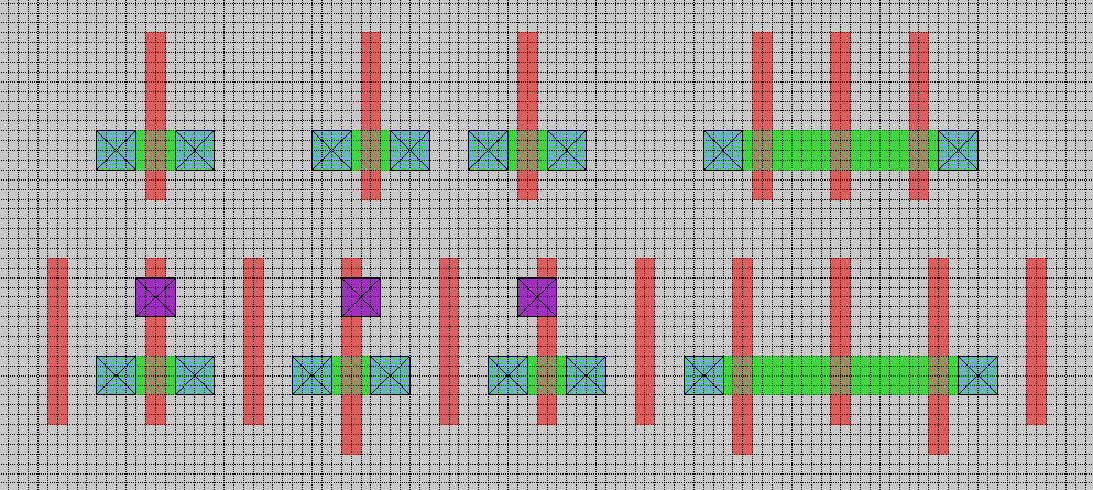
Figure 1. Example polysilicon-based structures which (top row) satisfy traditional MOSIS rules, and (bottom row) functionally identical ones which satisfy the "Special Nanometer-scale Rules for EEC 116."
                                  100λ max
                        |<--------------------------->|

                                    (poly)
                        X*****************************<Destination
                        |
  Driver>---------------X**********X------------------<Destination
               (metal)      (poly)       (metal)
Draw nwells around all PMOS transistors and pwells around all NMOS transistors and connect them to Gnd or Vdd as appropriate.
Place at least one nwell/psubstrate contact for every 3 squares of nwell/pwell. ("squares" in this context is not referring to the lambda grid shown in magic. Rather, it refers to a square of material with its length equal to its width, as discussed under the topic of sheet resistance near the midpoint of the course. Thus, in typical orientation with nwell and pwell having a wide and short aspect, a section of 3 squares of well would have a width three times as wide as its height.)
Polysilicon may be oriented in only one direction for the entire chip. [all transistors in same direction, in one tech. began at 45 nm], [no horizontal poly, in one tech. began at 32 nm]
Polysilicon spacing along its long edge may be only
a) 8 λ, or
b) greater than 16 λ unless stated
otherwise.
(Note: a space of 18 λ has the same overall pitch as layout
which uses dummy poly.)
Normal 3 λ minimum spacing rules apply along the shorter edges.
[all transistors on a pitch (approximately 2 lambda
poly width, 6 lambda spacing);
in one tech. began at 45 nm]
All polysilicon that is used for a functional circuit must have other polysilicon at a distance of 8 λ the entire length of both of its long edges. This implies the need for "dummy" unused poly in some cases. See Fig. 1. [dummy poly on each side of each poly, in one tech. began at 45 nm], [two dummy polys on each side of each poly that matters (designer put one dummy poly on each side in the INV cell); in one tech. began at 32 nm]
Exceptions:
Rule #4.3 may be violated for a maximum length of 3 λ as shown in three examples in Fig. 1.
Rule #4.3 may be violated for polysilicon-to-metal contacts but the poly contact may extend beyond the poly "wire" by a maximum of 2 λ as shown in Fig. 1.
Figure 1. Example polysilicon-based structures which (top row) satisfy traditional MOSIS rules, and (bottom row) functionally identical ones which satisfy the "Special Nanometer-scale Rules for EEC 116."
2010/11/22  Posted
2010/11/23  Added nwell/pwell rules
2010/11/24  Corrected rule 3.4 to 16 lambda, not 12 lambda
2013/10/14  Added detail to ascii figure for polysilicon rule
2013/11/21  Added examples of exceptions to rule #2 in Figure 1,
            and minor tweaks to polysilicon ascii figure
2014/10/23  Moved poly width to rule #2, plus other reorganization
2014/11/04  Fixed typo: 4.4 should have been 4.3
2017/11/28  Fixed minor typo
2018/11/12  Added several references to specific technology generations
2019/11/01  Clarified rule 4.2 applies to only the long edges of poly
2020/10/20  Minor clarification regarding sheet resistance squares