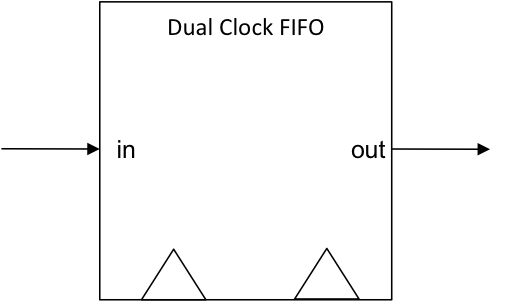
Simplified view of dual clock FIFO.
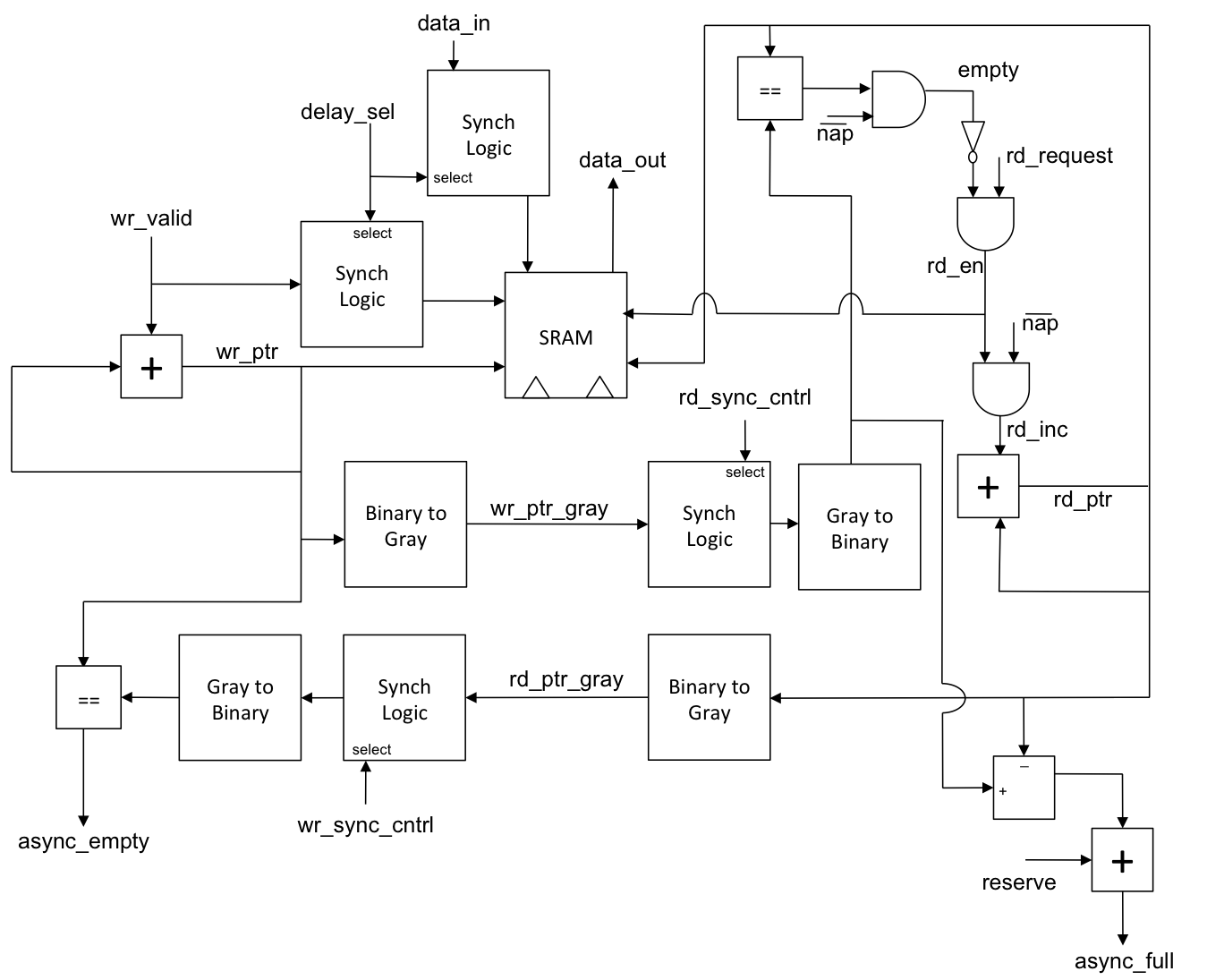
Block diagram of the dual clock FIFO.
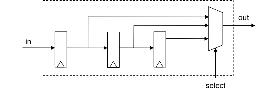
Diagram showing the synch logic used in the previous block diagram.
This dual clock FIFO is designed as a way for two circuits operating in different clock frequencies to communicate with each other. There is a read side and write side where data is stored into the internal memory of the FIFO using the write side clock and then read from the internal memory using the read side clock. This module is meant to be flexible, allowing to easily change the data width and address width as well as the size of the internal memory.
This project was motivated by the need for a simple dual clock FIFO similar to the dual clock FIFO designed by Ryan Apperson which is used inside of the VCL group's AsAP2 chip. To make this design Ryan's thesis was used as a guide. For completeness sake there is extra circuitry and signals specifically meant to be used by the AsAP2 chip. It was desirable to have a single module that was straightforward and easy to change.
A testbench was created to test this circuit which will randomly choose a clock frequency for each clock after each clock pulse. Each side will randomly stop reading or writing accordingly for a random amount of clock pulses. The output is monitored and it will give an error if a non sequential output is given, which would mean an incorrect value was read.
For additional information and/or suggestions email: astillmaker -a,t- ucdavis -period- edu