|
Fall 2024
|
See your name here!
|
|
Fall 2023
|
|
Project:
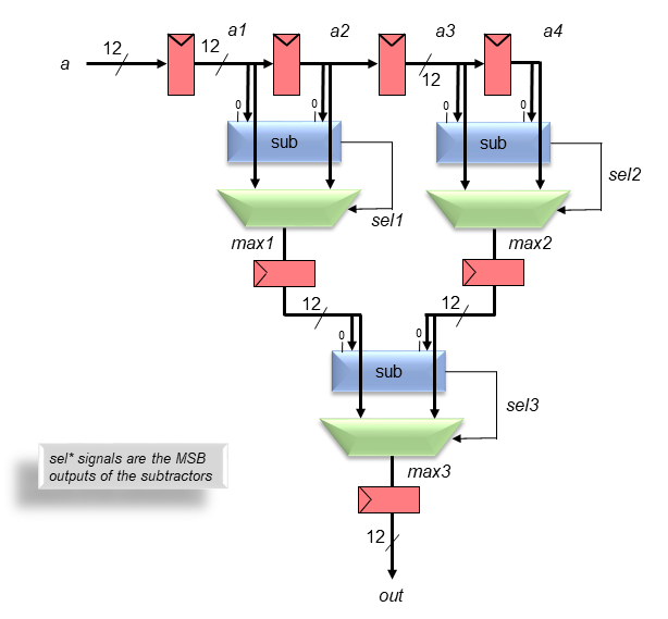
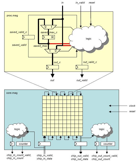
This project consists of the design and layout of a chip which finds
the maximum value among the last four 12-bit numbers to enter the chip.
It is a type of sliding window filter often used in digital signal
processing workloads.
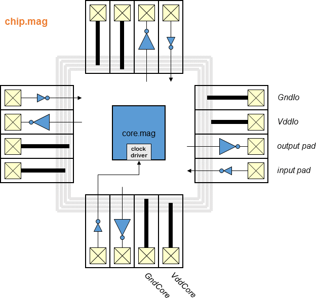
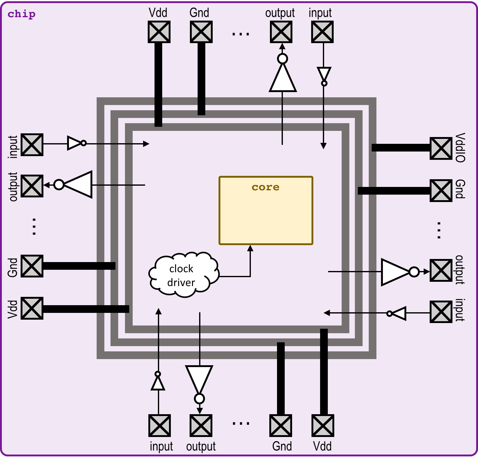
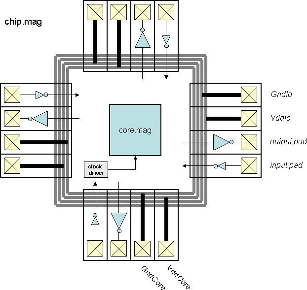
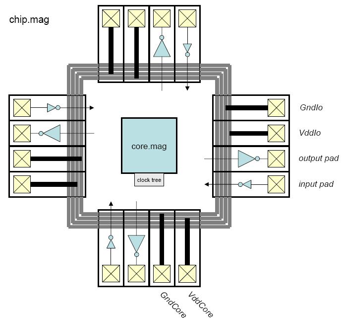
Chips include clock trees, power rings and grid, Vdd/Gnd/input/output
I/O pads with the output pad sufficient for driving a 10 pF load.
Students produced all layout themselves.
The chips were laid out using TSMC's 0.18 μm CMOS and scalable
design rules.
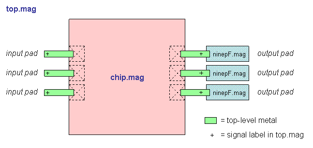
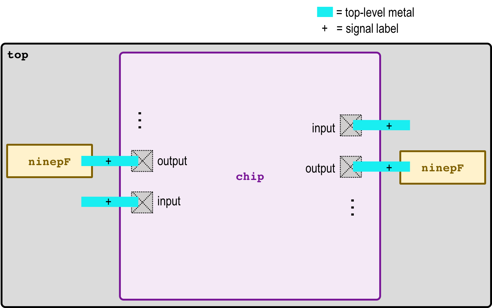
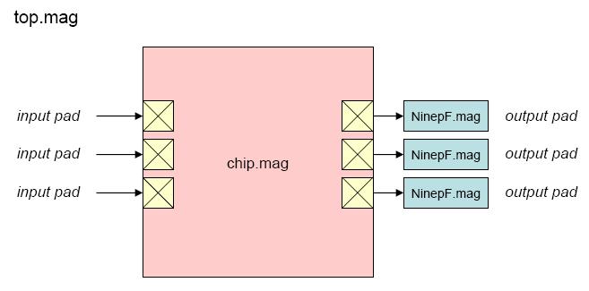
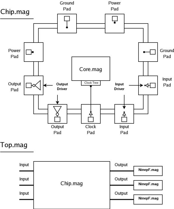
"Top" is the highest-level test environment
that includes the complete chip and 10 pF loads on all outputs.
|
- Block diagram (chip)
- Block diagram (top)
|
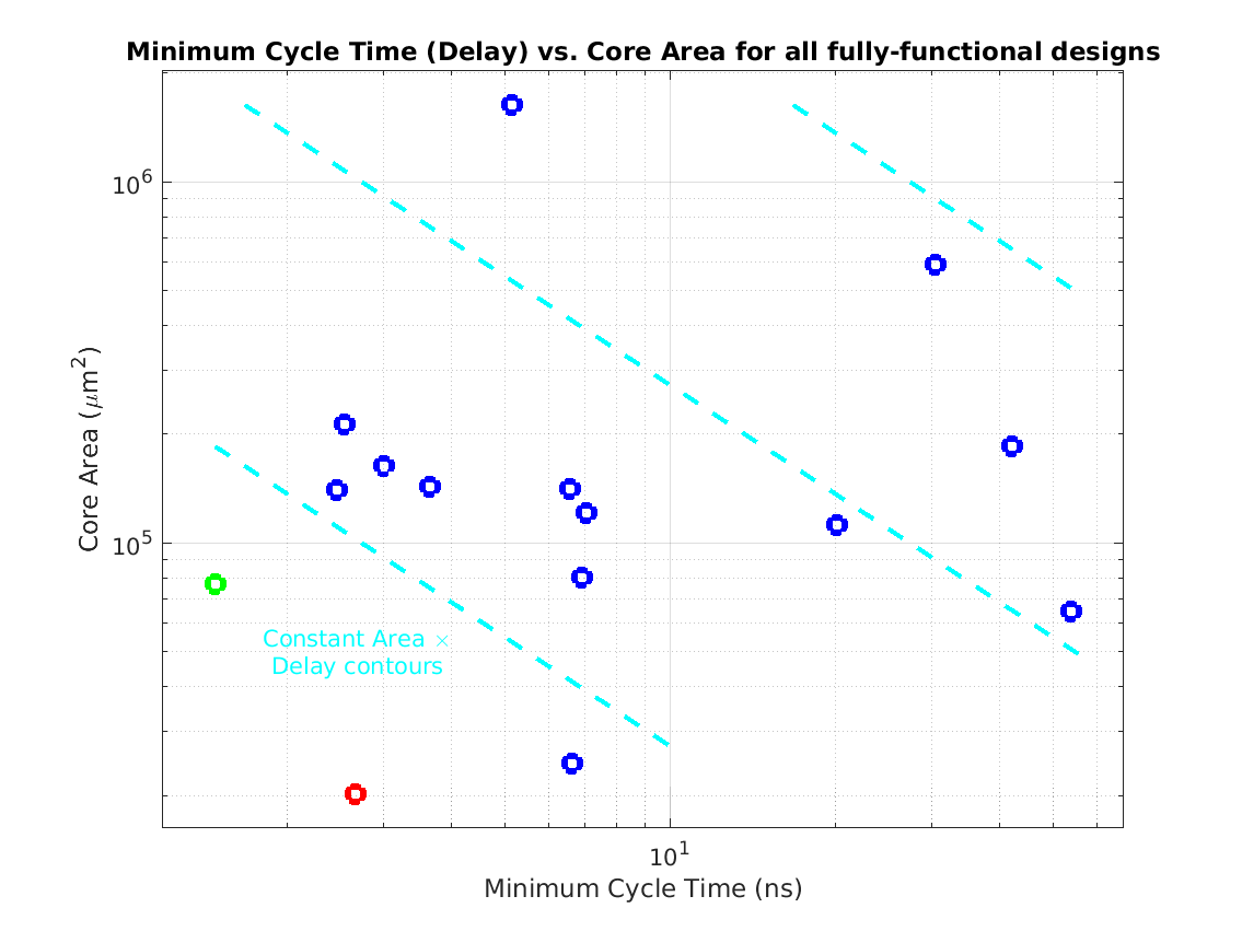
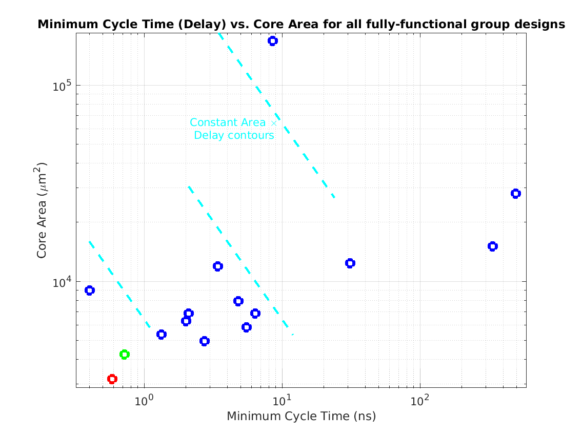
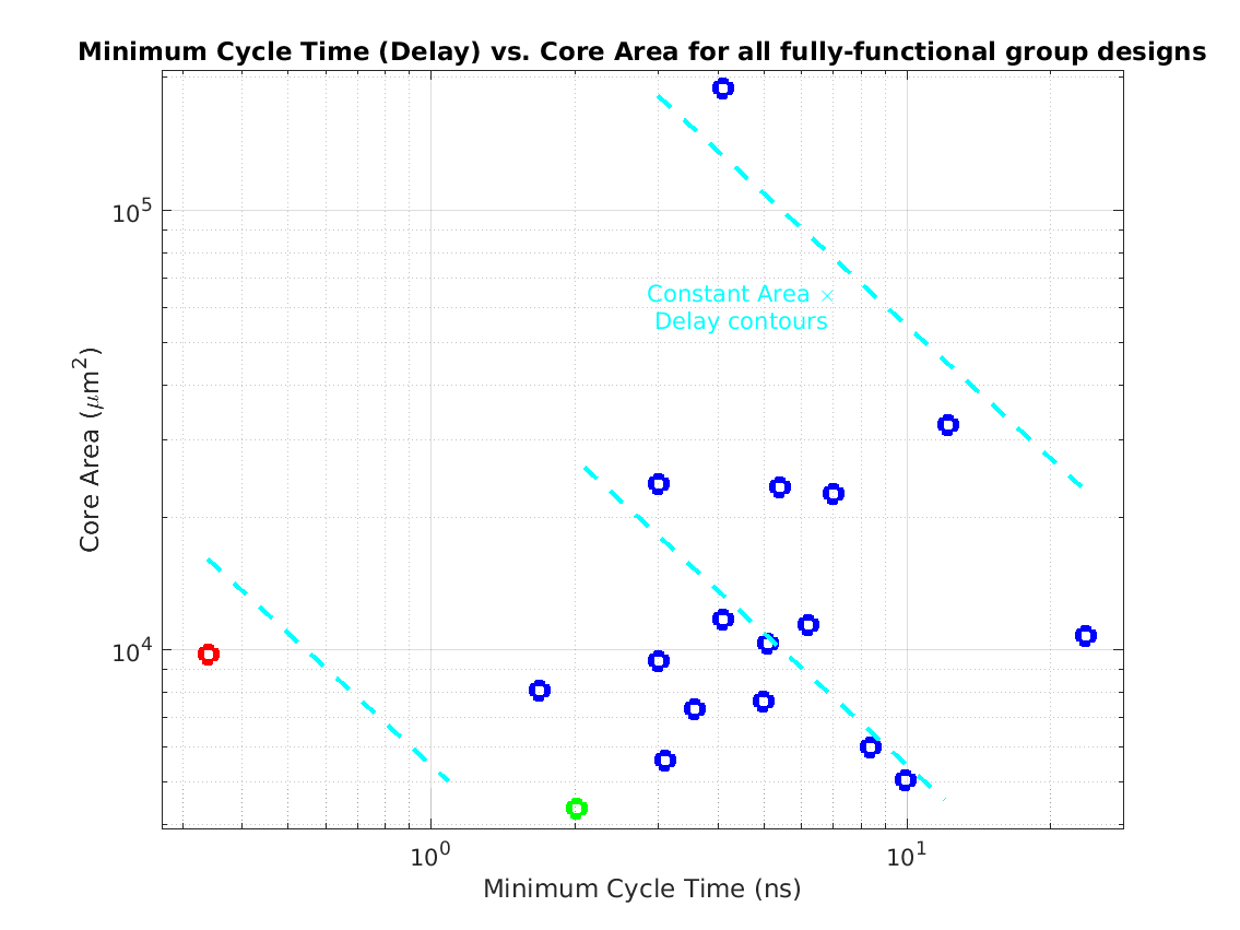
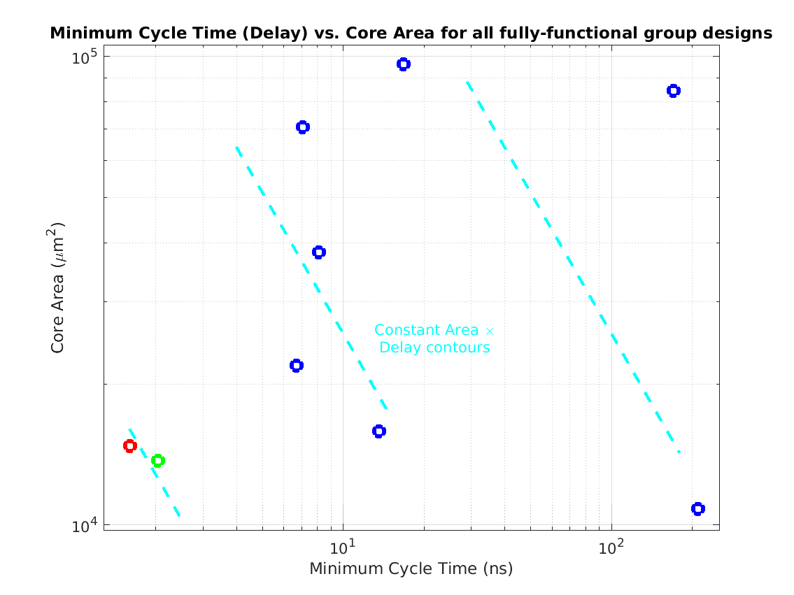
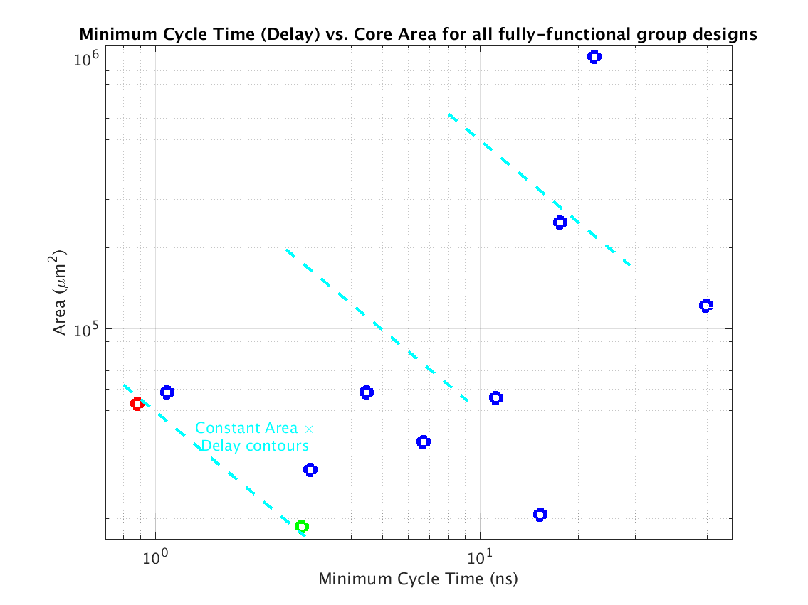
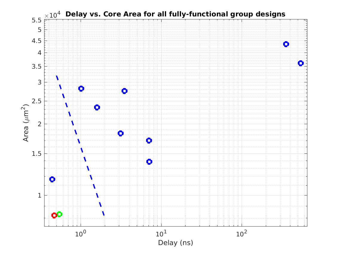
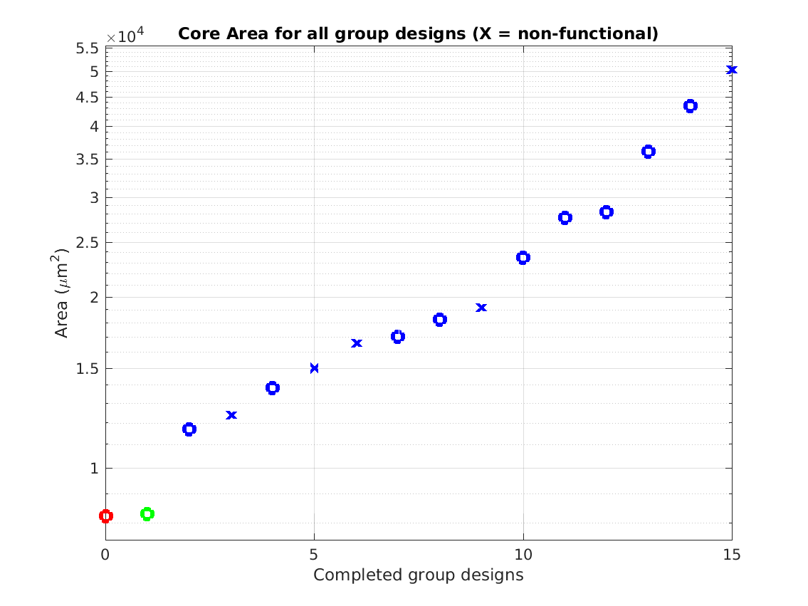
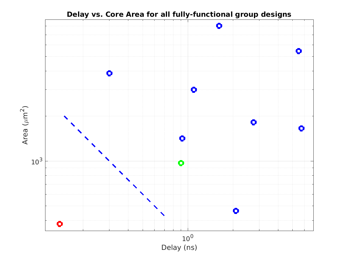
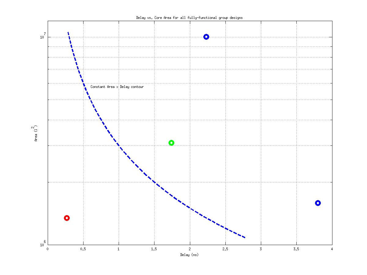
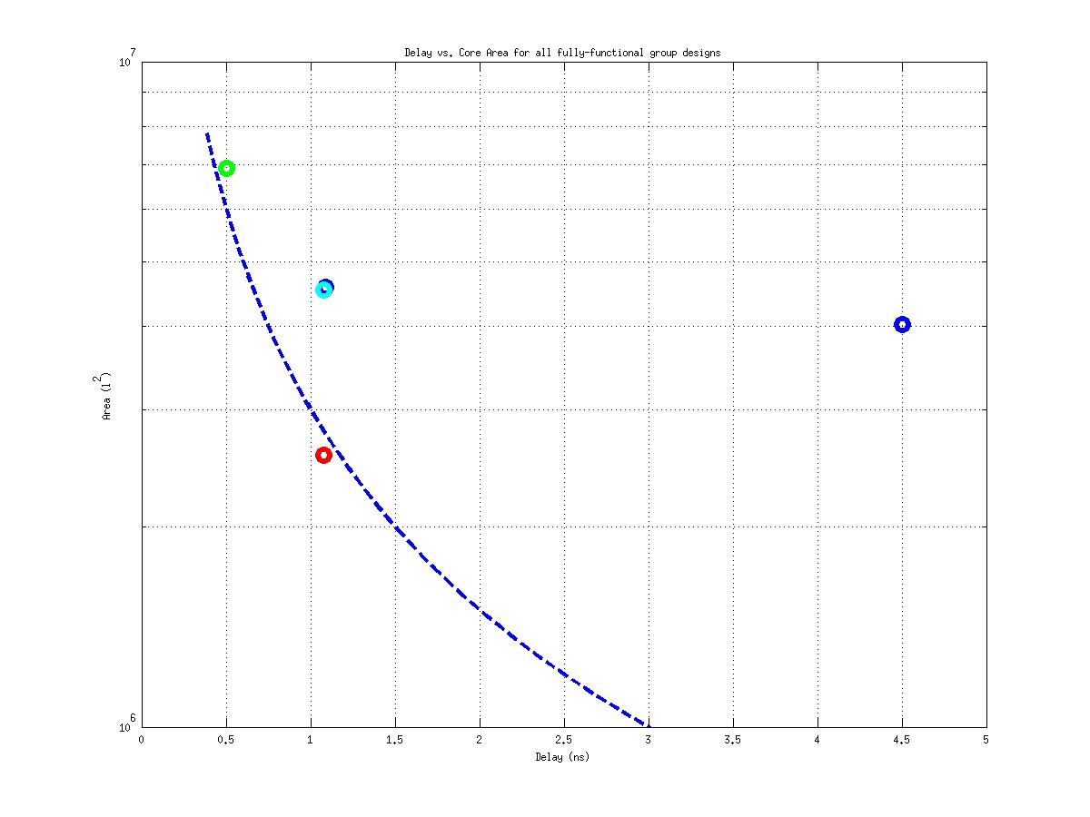
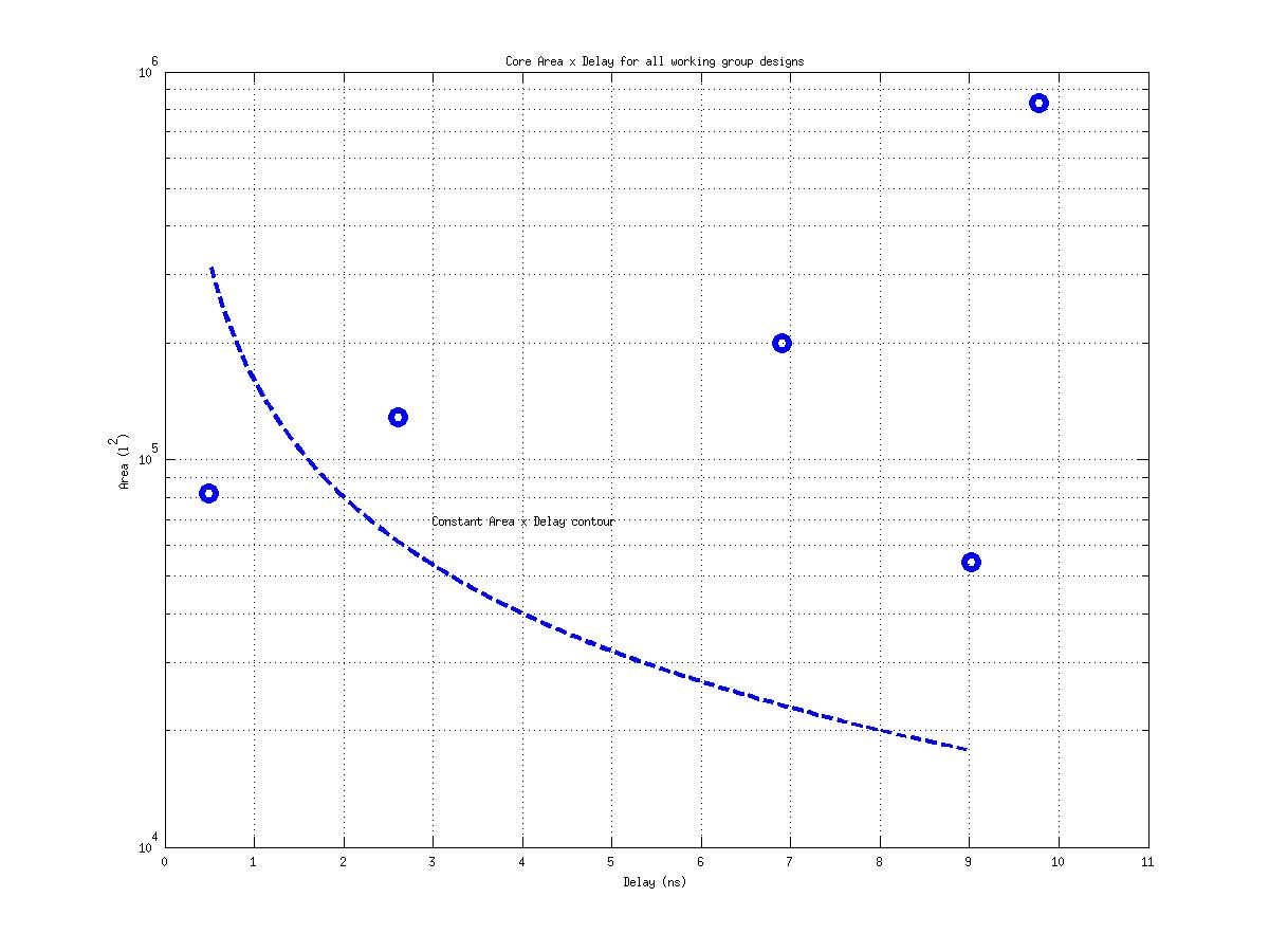
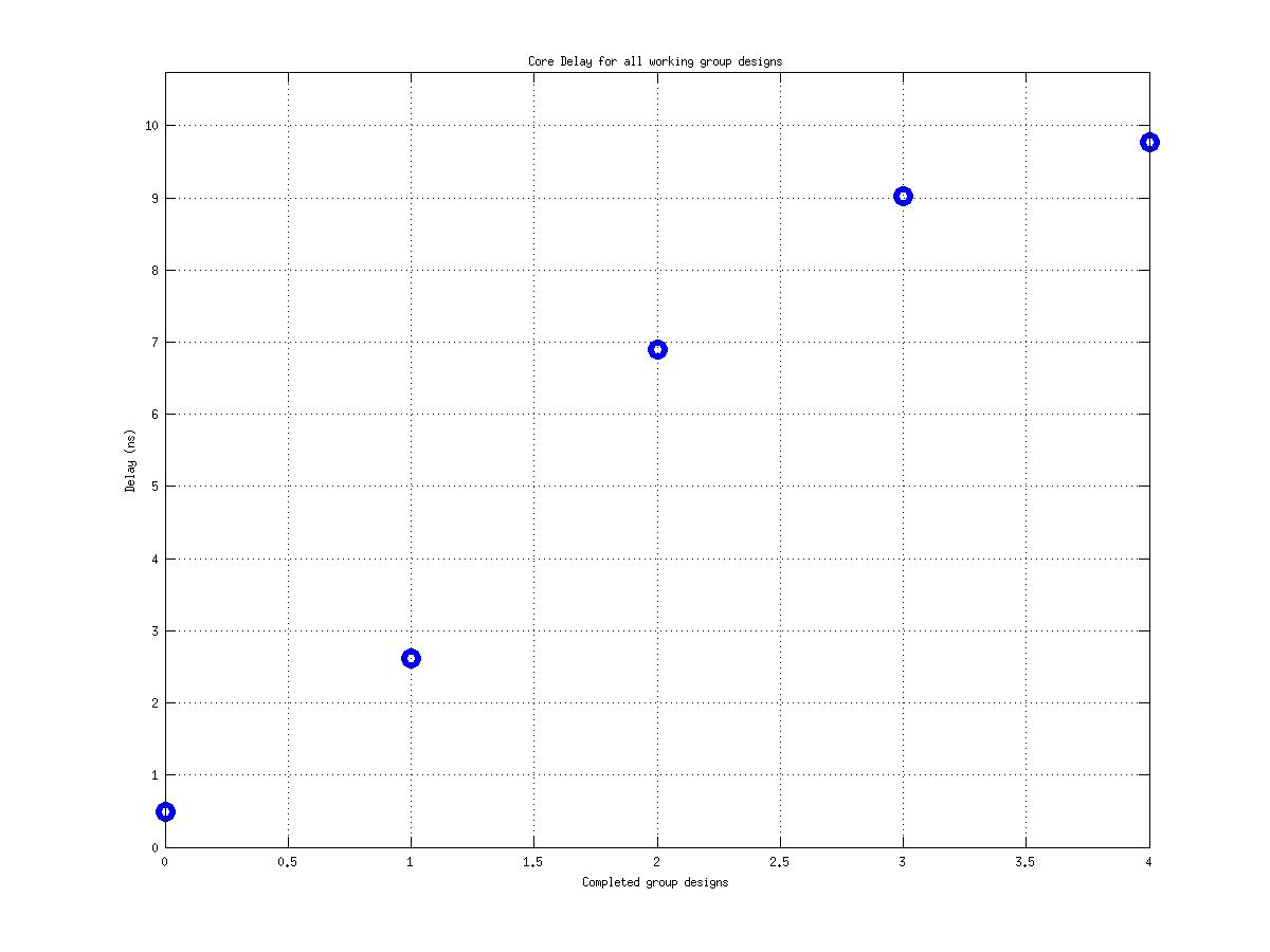
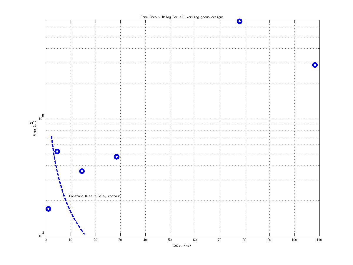
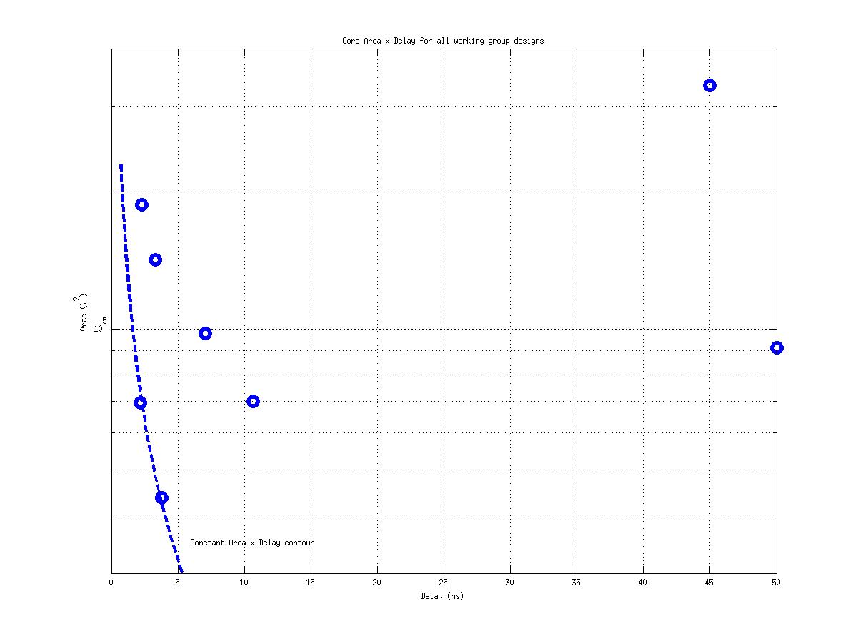
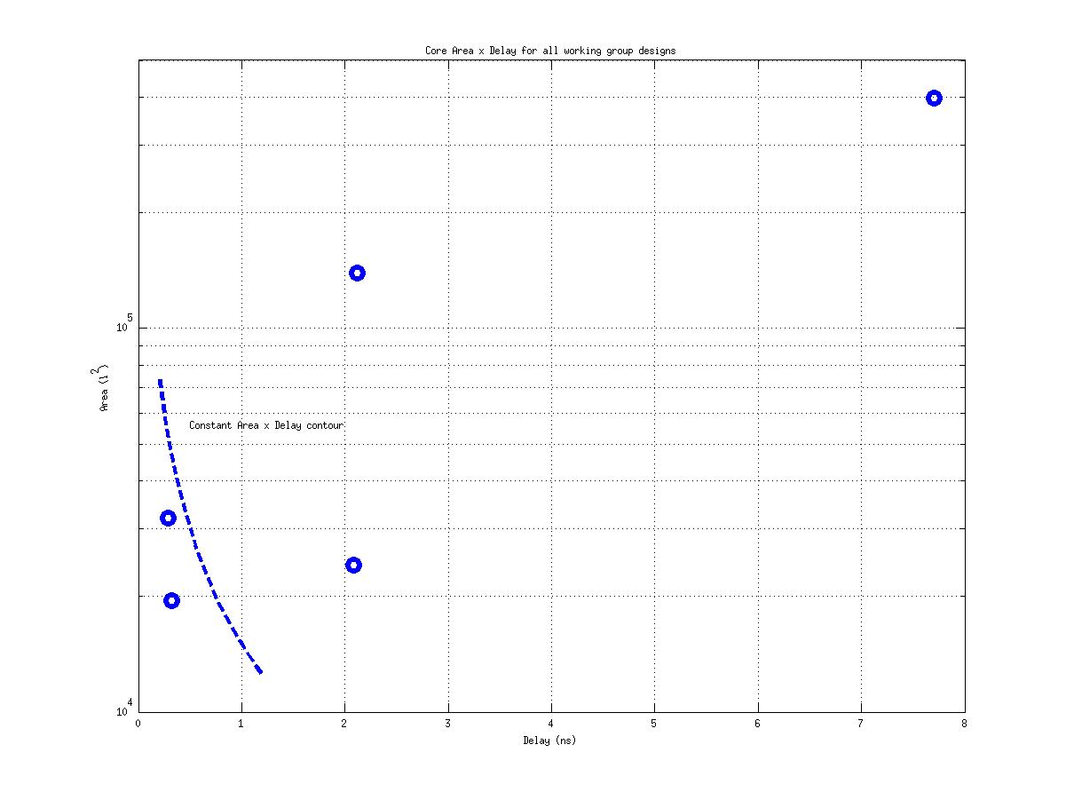
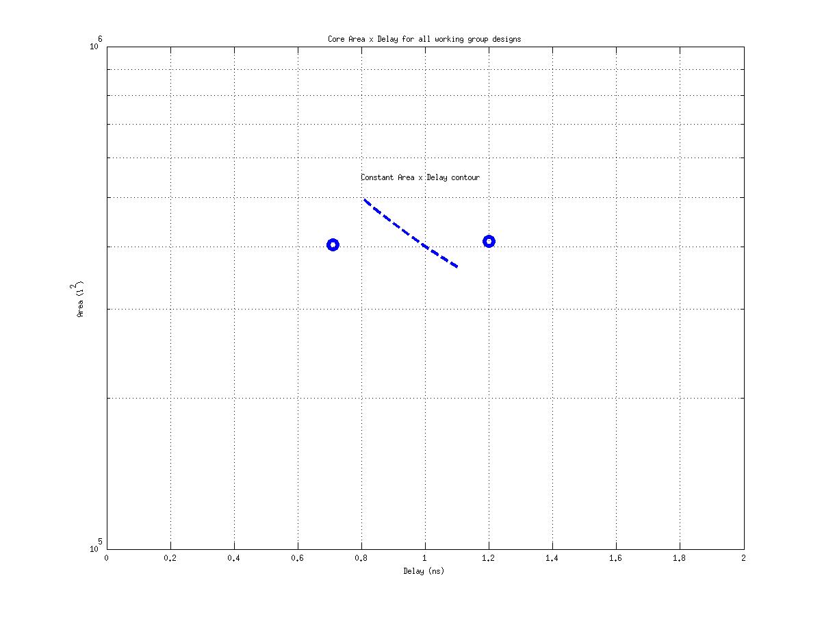
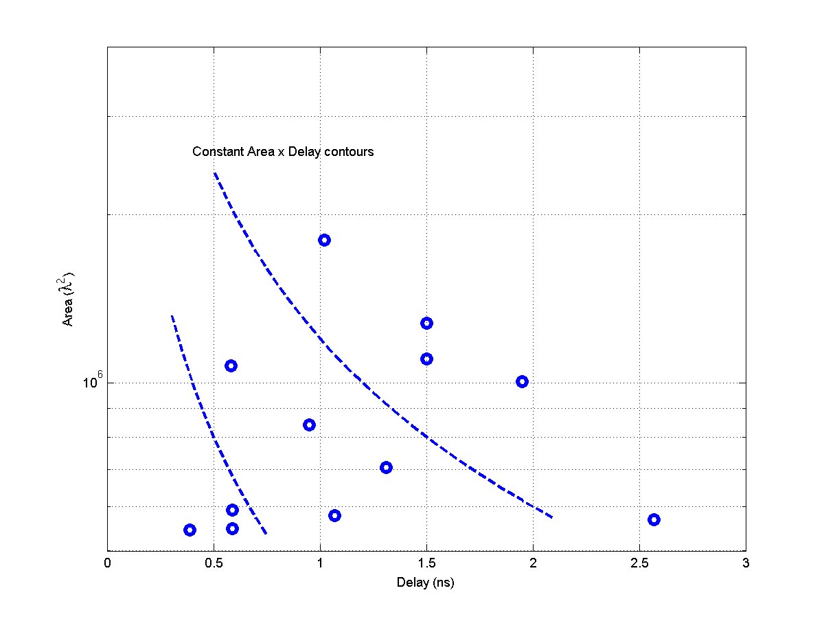
Class: Area × Minimum Cycle Time (Delay)
|
|
| |
Min: |
53,955 μm2⋅ns
|
| |
Max: |
17,964,692 μm2⋅ns
|
| |
Median: |
554,862 μm2⋅ns
|
| |
Ratio max/min: |
333! |
|
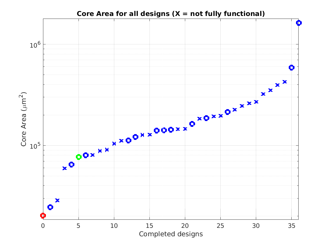
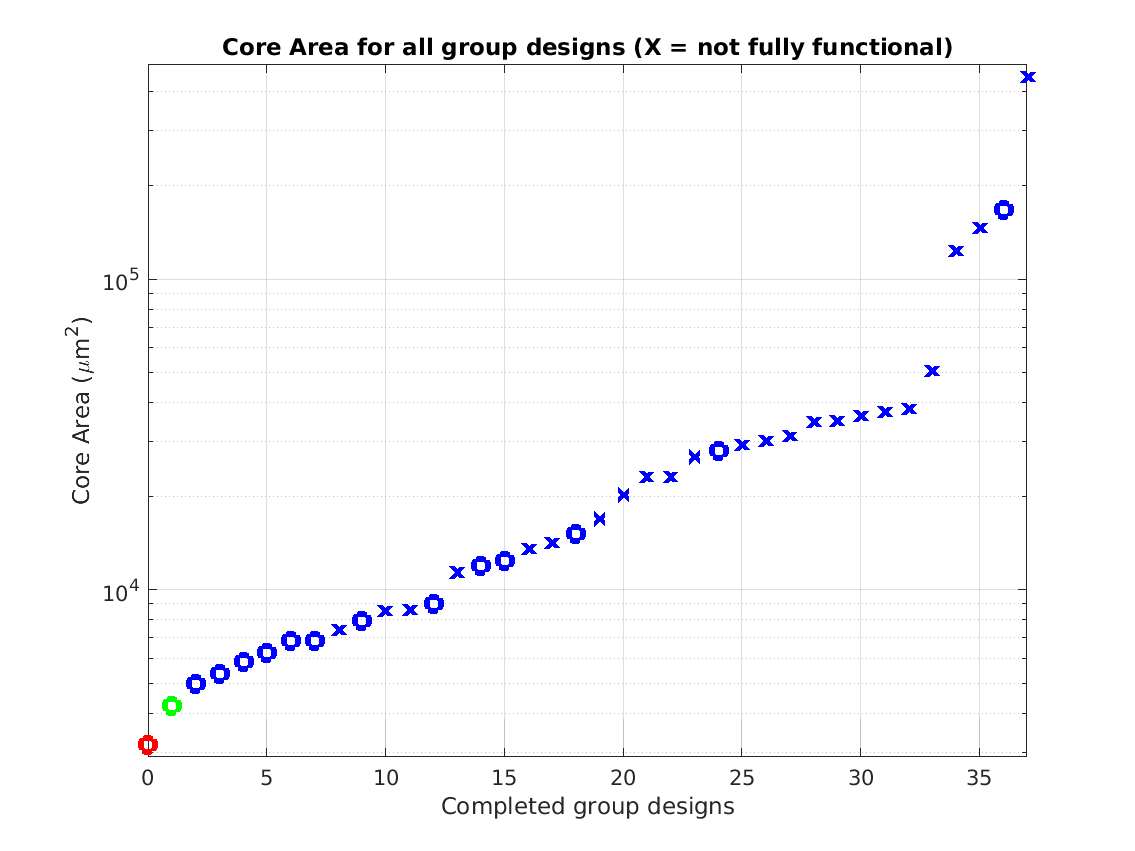
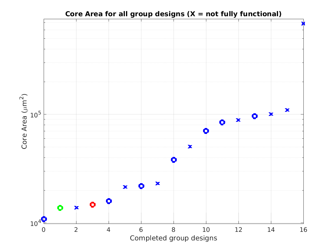
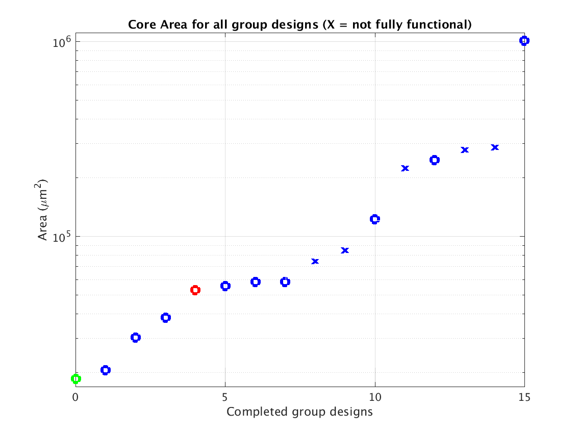
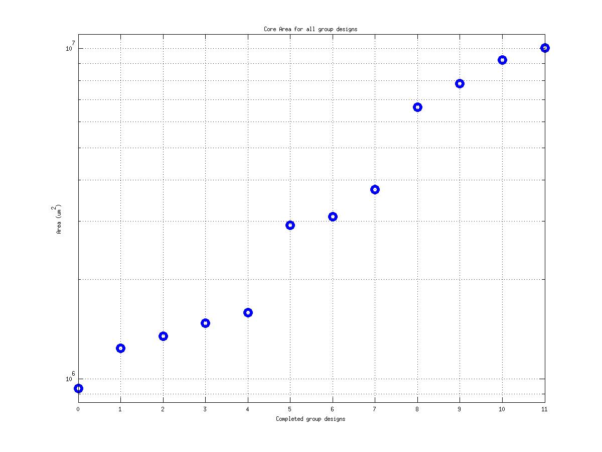
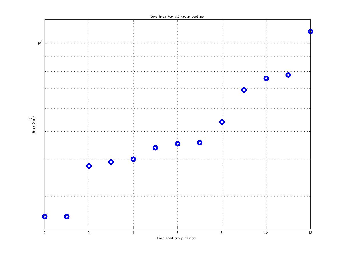
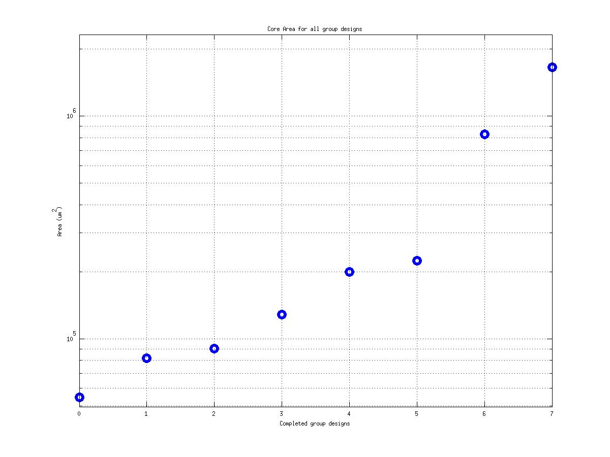
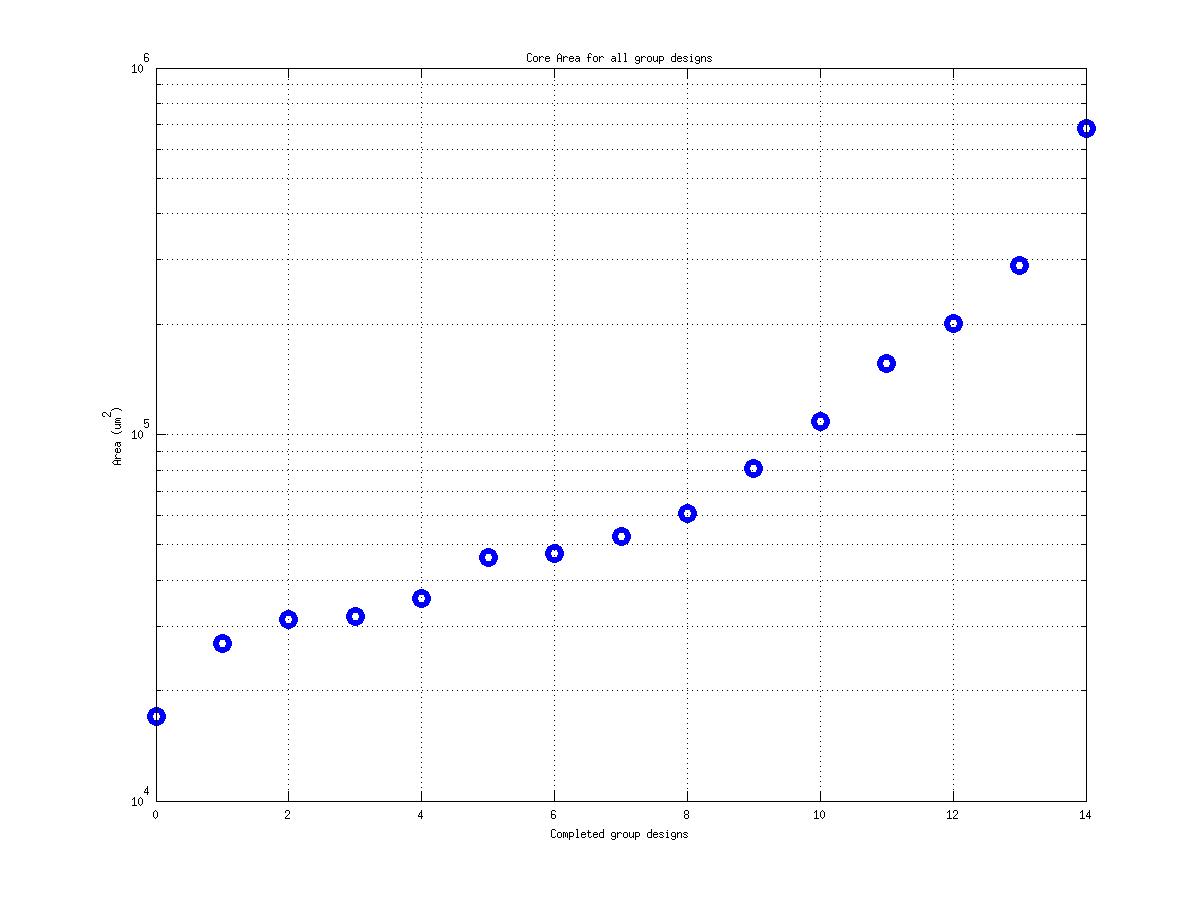
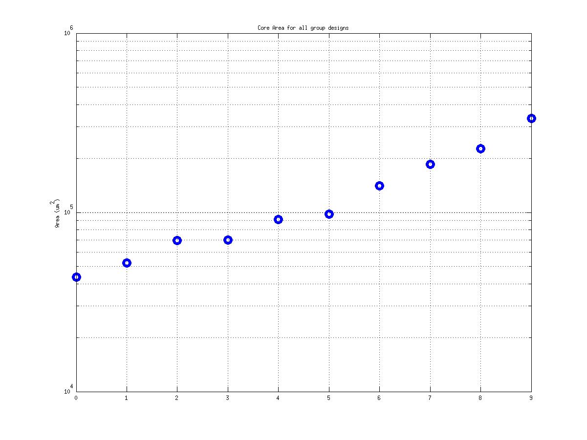
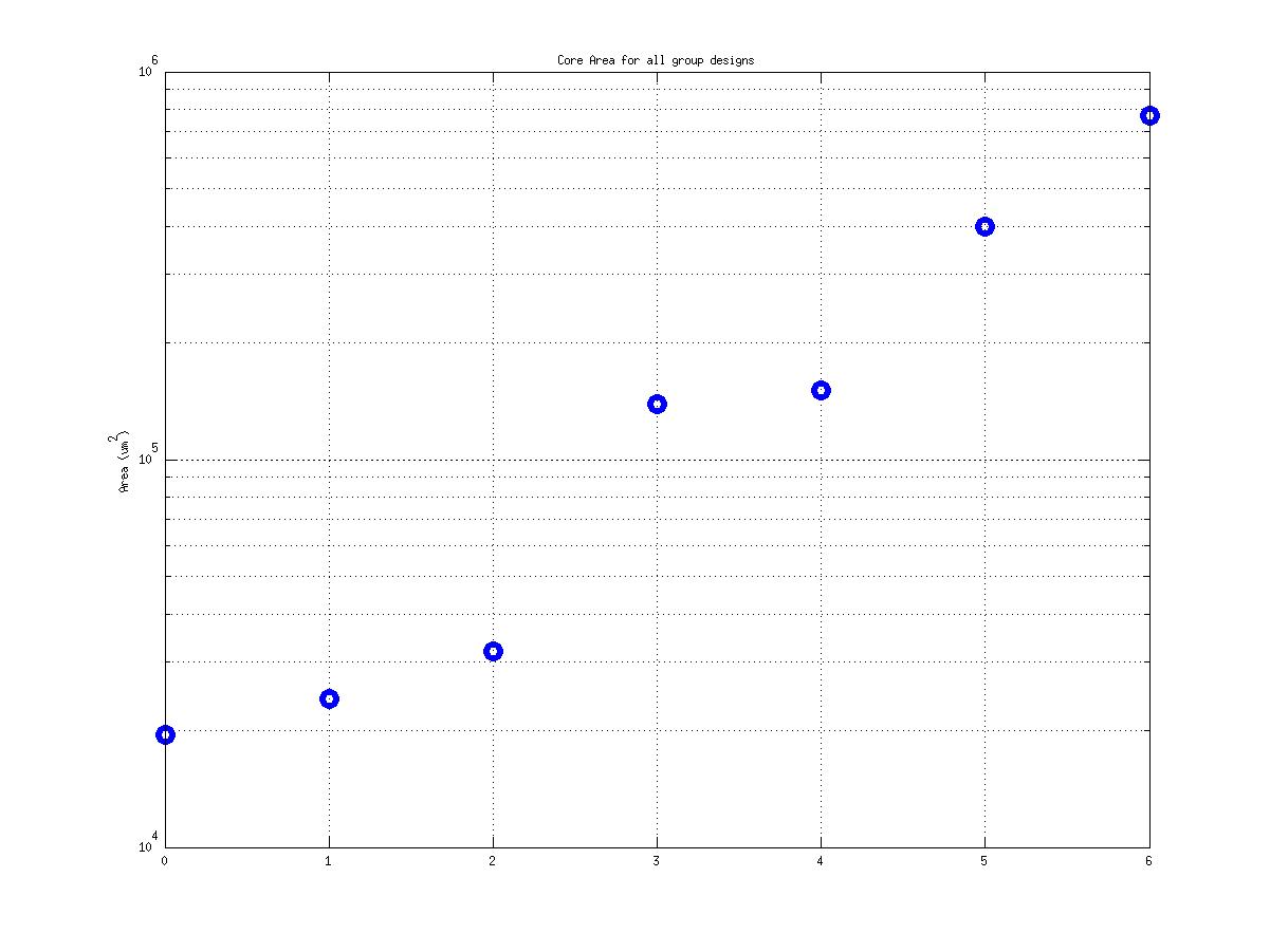
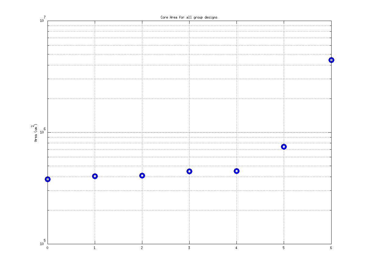
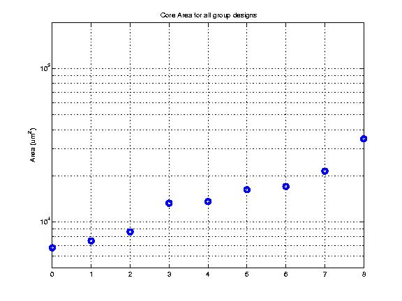
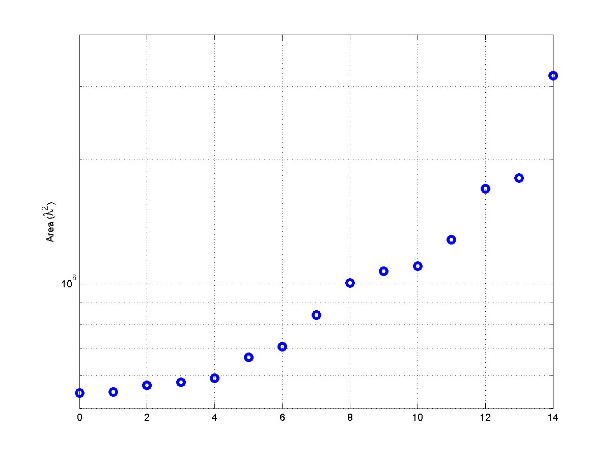
Class: core.mag Area
|
|
| |
Min: |
20,284 μm2 |
| |
Max: |
1,631,667 μm2
|
| |
Median: |
143,444 μm2
|
| |
Ratio max/min: |
80! |
|
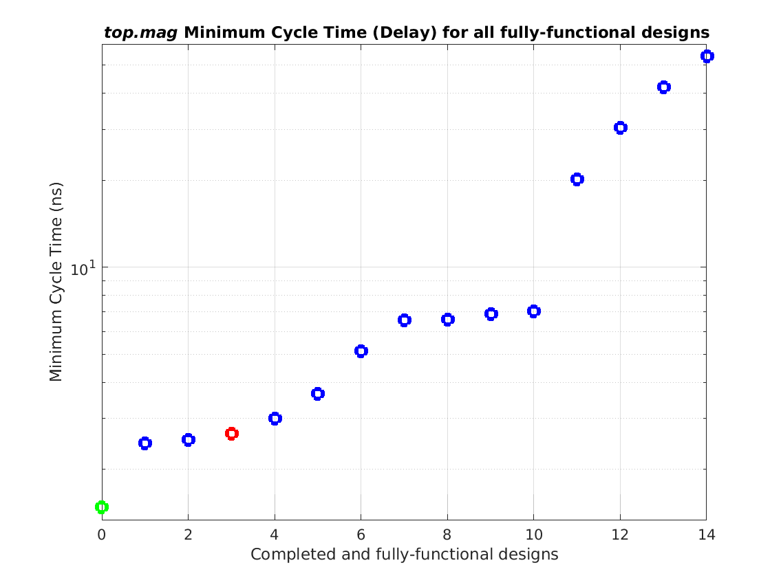
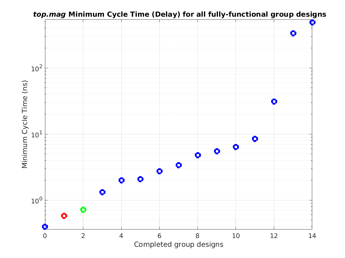
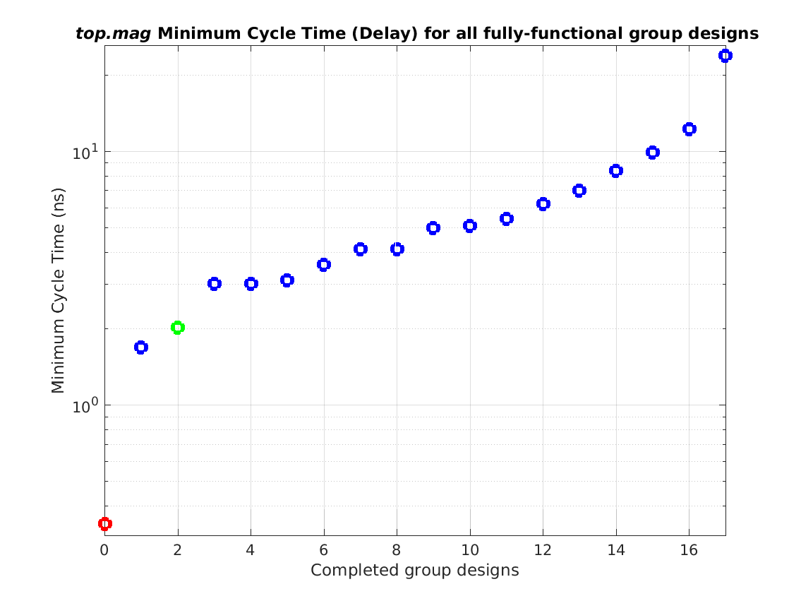
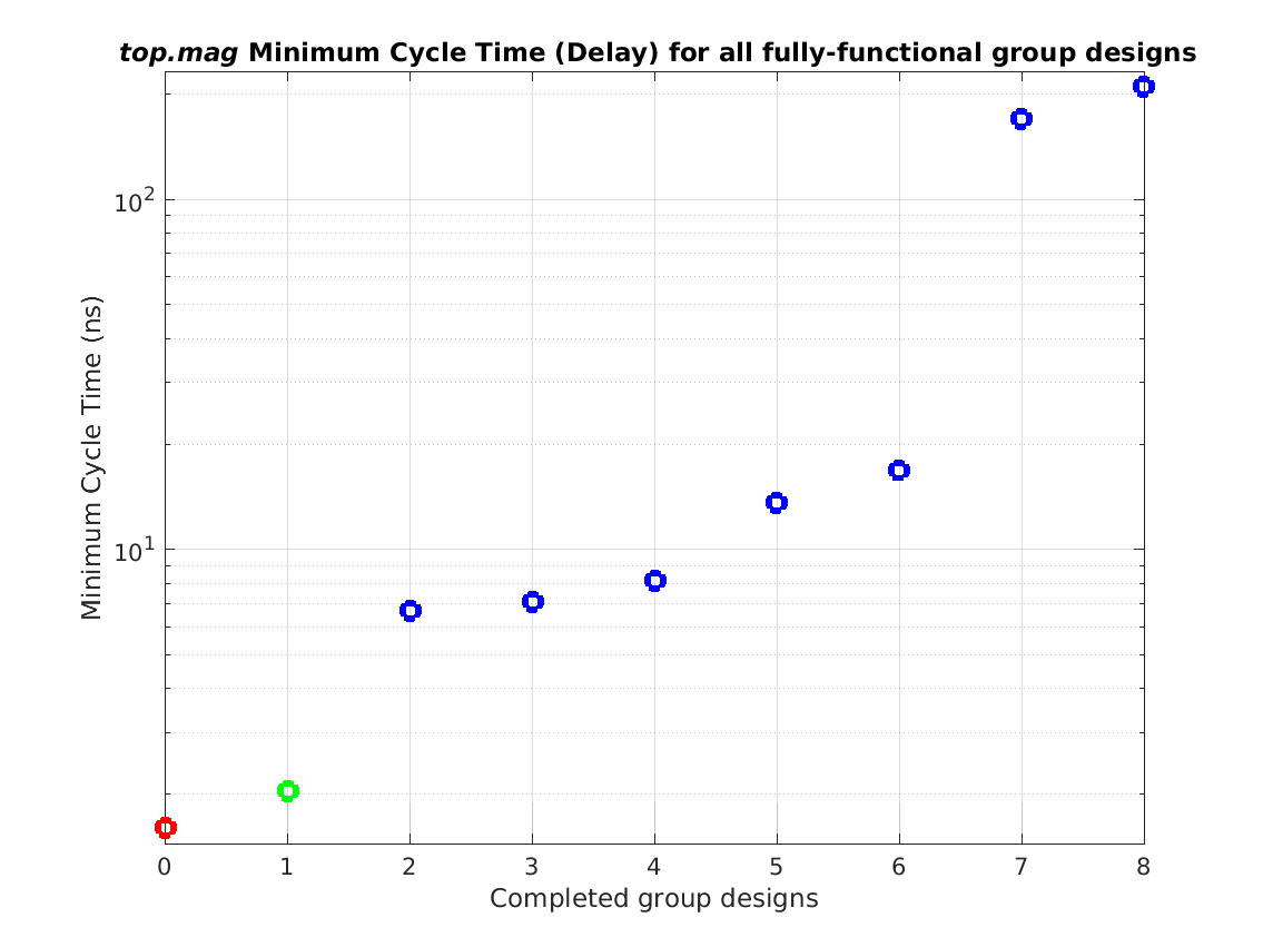
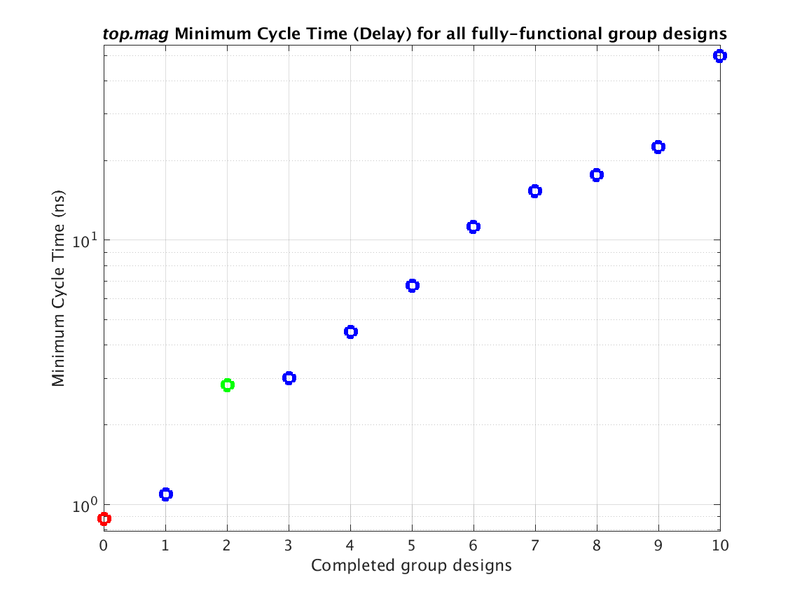
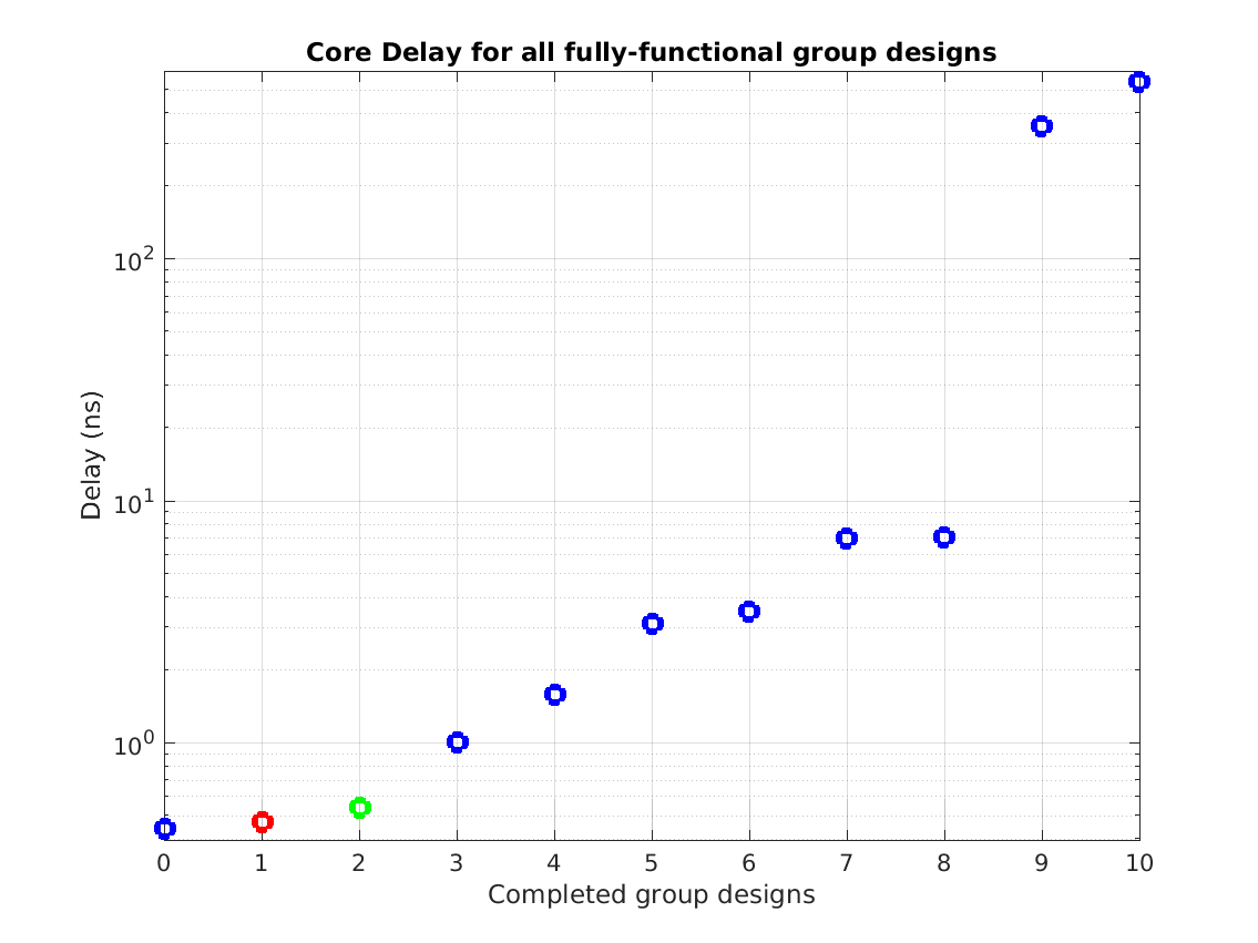
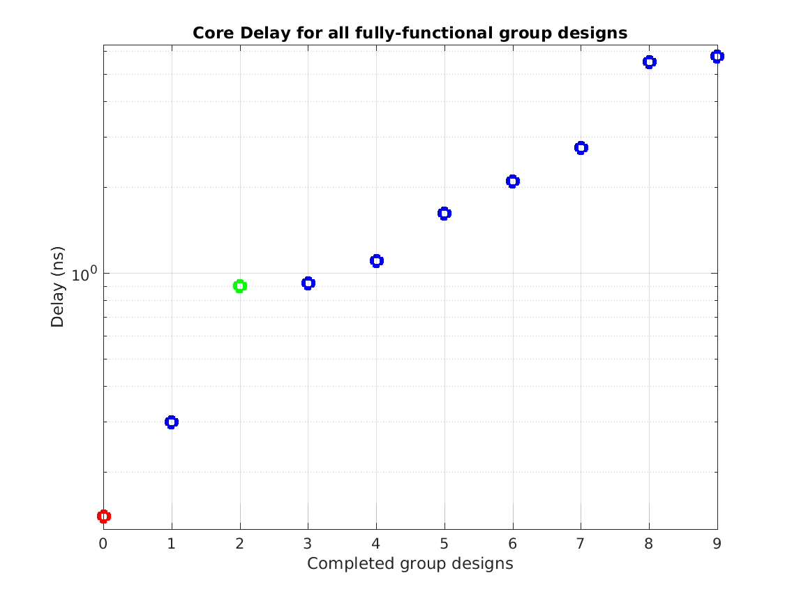
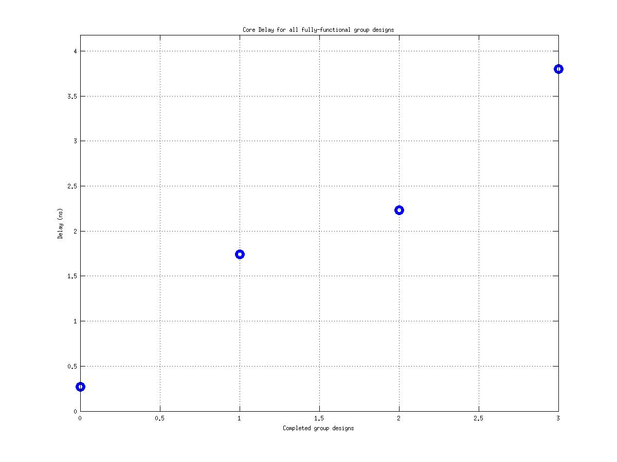
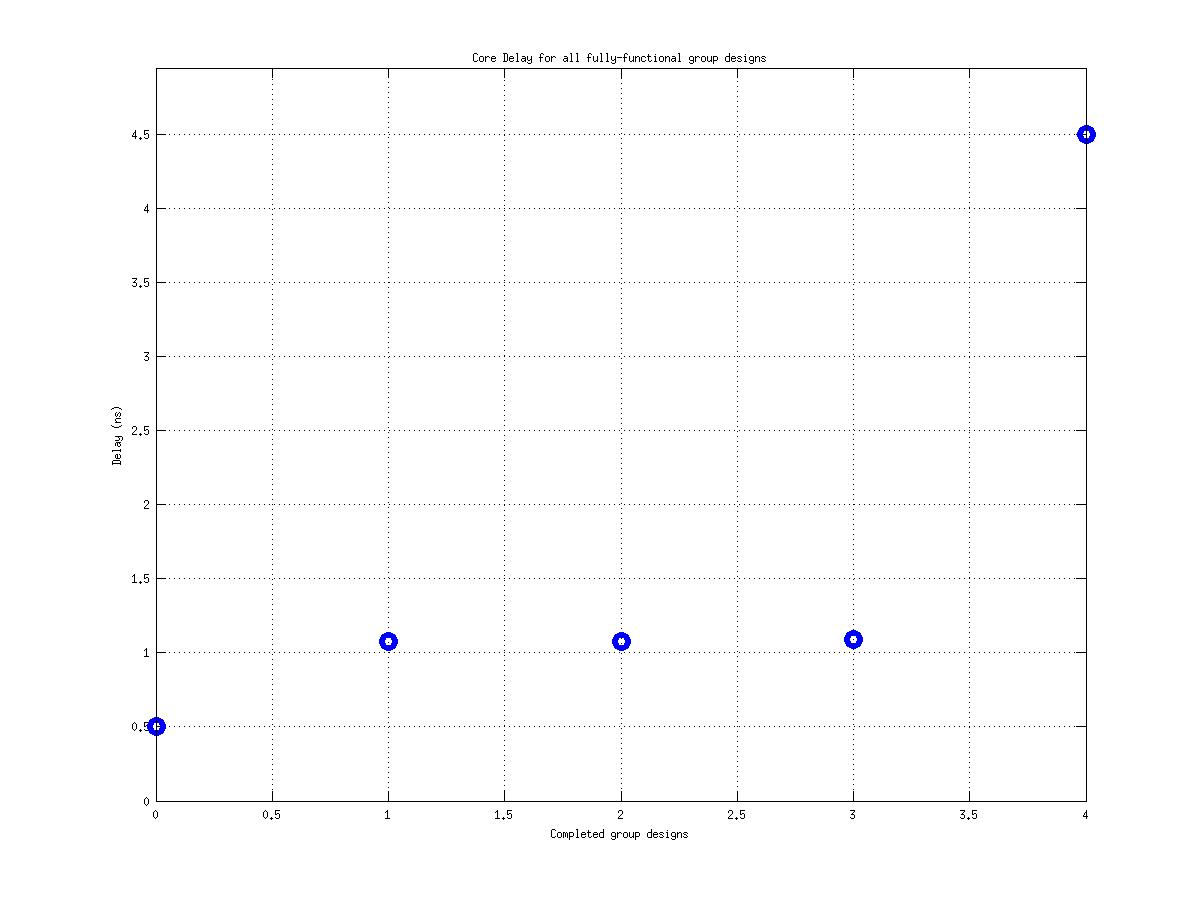
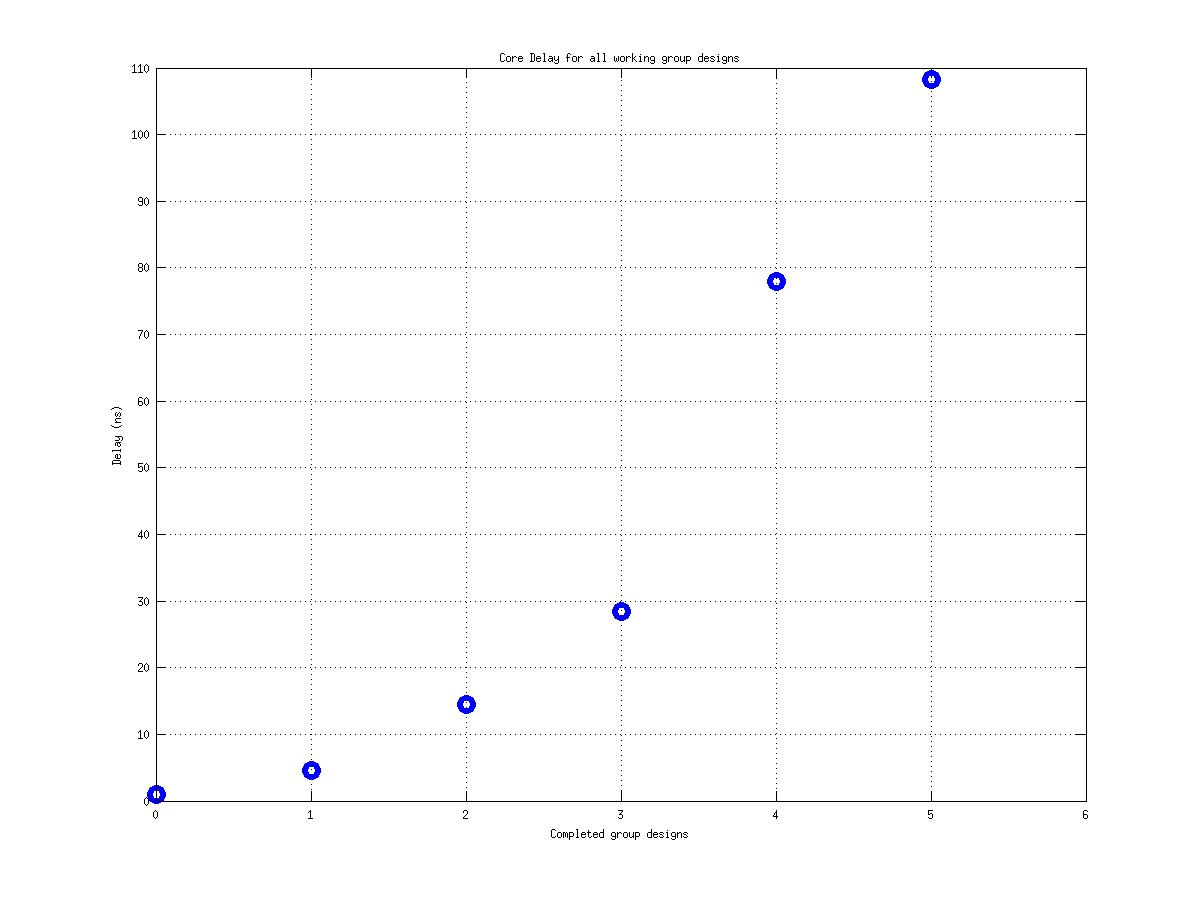
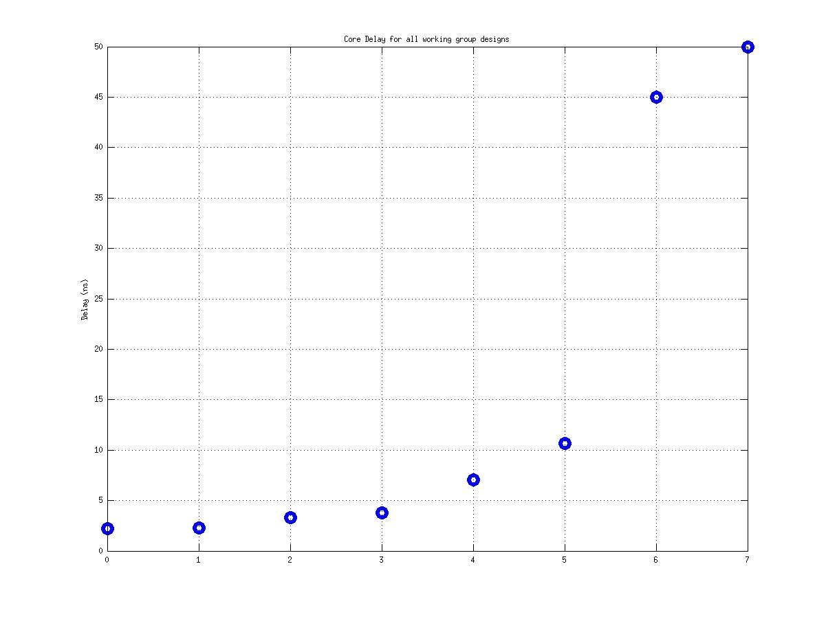
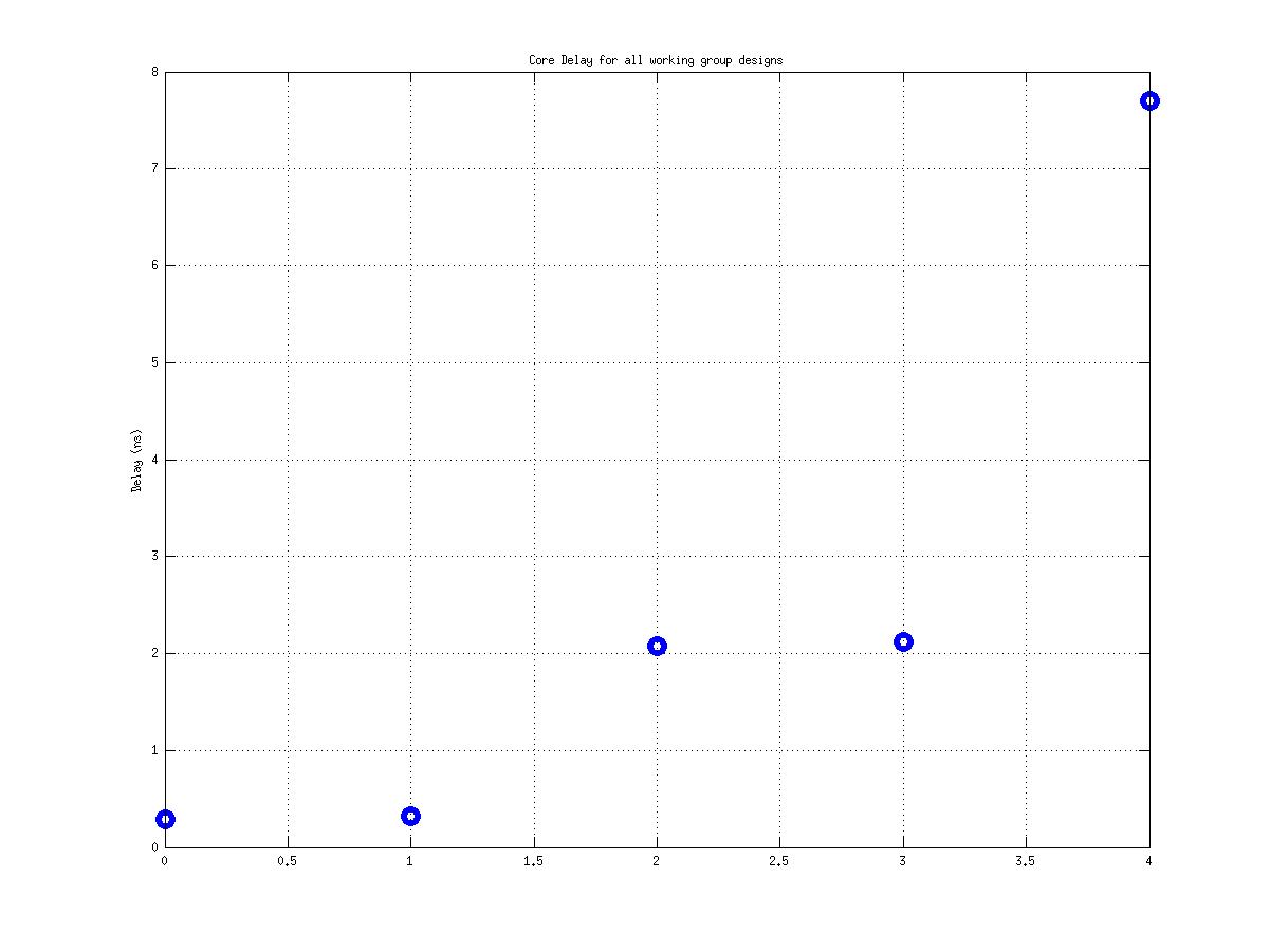
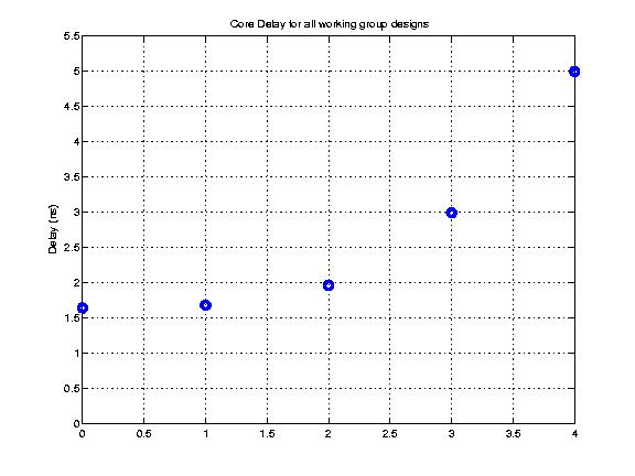
Class: top.mag Minimum Cycle Time (Delay)
|
|
| |
Min: |
1.48 ns |
| |
Max: |
53.83 ns |
| |
Median: |
6.56 ns |
| |
Ratio max/min: |
36! |
|
|
First place winner
|
| |
Chip core (shown to scale with 2nd place) |
Entire chip |
Jordan Ricci
Area × Delay
= 53,995 μm2⋅ns
Core Area
= 20,284 μm2
Top-level Min Cycle Time = 2.66 ns
(376 MHz)
|
![[core]](23/ricci-core.211wide.png)
|
![[chip]](23/ricci-chip.250wide.png)
|
|
Second place winner
|
| |
Chip core (shown to scale with 1st place) |
Entire chip |
Michael Wang
Area × Delay
= 114,355 μm2⋅ns
Core Area = 77,267 μm2
Top-level Min Cycle Time = 1.48 ns
(676 MHz)
|
![[core]](23/wang-core.300wide.png)
|
![[chip]](23/wang-chip.250wide.png)
|
| |
|
Fall 2021
|
|
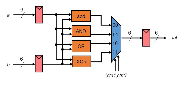
Project:
This project consists of the design and layout of a chip which calculates
the sum, bitwise AND, bitwise OR, and bitwise XOR of two 6-bit inputs. A
6-bit 4:1 multiplexer selects which output is sent to the chip's output
pads.
Chips include clock trees, power rings and grid, Vdd/Gnd/input/output
I/O pads with the output pad sufficient for driving a 10 pF load.
Students produced all layout themselves.
The chips were laid out using TSMC's 0.18 μm CMOS and scalable
design rules.
"Top" is the highest-level test environment
that includes the complete chip and 10 pF loads on all outputs.
|
- Block diagram (chip)
- Block diagram (top)
|
Class: Area × Minimum Cycle Time (Delay)
|
|
| |
Min: |
1,859 μm2⋅ns
|
| |
Max: |
13,821,462 μm2⋅ns
|
| |
Median: |
32,197 μm2⋅ns
|
| |
Ratio max/min: |
7433! |
|
Class: core.mag Area
|
|
| |
Min: |
3,184 μm2 |
| |
Max: |
447,473 μm2
|
| |
Median: |
16,046 μm2
|
| |
Ratio max/min: |
5 |
|
Class: top.mag Minimum Cycle Time (Delay)
|
|
| |
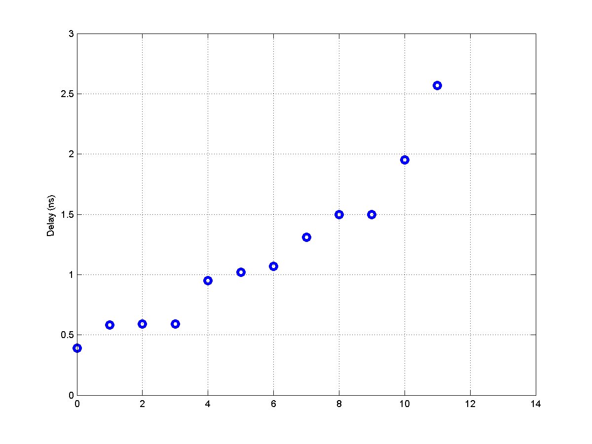
Min: |
0.40 ns |
| |
Max: |
493.8 ns |
| |
Median: |
3.40 ns |
| |
Ratio max/min: |
1234! |
|
|
First place winner
|
| |
Chip core (shown to scale with 2nd place) |
Entire chip |
Joseph Arbuckle
Area × Delay
= 1,859 μm2⋅ns
Core Area
= 3,184 μm2
Top-level Min Cycle Time = 0.58 ns
(1.72 GHz!)
|
![[core]](21/arbuckle-core.300wide.png)
|
![[chip]](21/arbuckle-chip.250wide.png)
|
|
Second place winner
|
| |
Chip core (shown to scale with 1st place) |
Entire chip |
Thomas Abbott
Area × Delay
= 3,057 μm2⋅ns
Core Area = 4,246 μm2
Top-level Min Cycle Time = 0.72 ns
(1.39 GHz)
|
![[core]](21/abbott-core.188wide.png)
|
![[chip]](21/abbott-chip.250wide.png)
|
| |
|
Fall 2020
|
|
Project:
This project consists of the design and layout of a chip which
accumulates the sum of a series of input numbers and also detects when the
10-bit input number is equal to zero, one, or two.
Due to the pandemic, chips were designed by students individually for the
first time however because of the extra experience, this will likely
continue in future years.
Chips include clock trees, power rings and grid, Vdd/Gnd/input/output
I/O pads with the output pad sufficient for driving a 10 pF load.
Students produced all layout themselves.
The chips were laid out using TSMC's 0.18 μm CMOS and scalable
design rules.
"Top" is the highest-level test environment
that includes the complete chip and 10 pF loads on all outputs.
|
- Block diagram (chip)
- Block diagram (top)
|
Class: Area × Minimum Cycle Time (Delay)
|
|
| |
Min: |
3,311 μm2⋅ns
|
| |
Max: |
773,379 μm2⋅ns
|
| |
Median: |
50,095 μm2⋅ns
|
| |
Ratio max/min: |
234! |
|
Class: core.mag Area
|
|
| |
Min: |
4,341 μm2 |
| |
Max: |
188,629 μm2
|
| |
Median: |
10,696 μm2
|
| |
Ratio max/min: |
44 |
|
Class: top.mag Minimum Cycle Time (Delay)
|
|
| |
Min: |
0.34 ns |
| |
Max: |
23.7 ns |
| |
Median: |
4.54 ns |
| |
Ratio max/min: |
70! |
|
|
First place winner
|
| |
Chip core (shown to scale with 2nd place) |
Entire chip |
Tyler Sun
Area × Delay
= 3,311 μm2⋅ns
Core Area
= 9,739 μm2
Top-level Min Cycle Time = 0.34 ns
(2.94 GHz!)
|
![[core]](20/sun-core.269wide.png)
|
![[chip]](20/sun-chip.250wide.png)
|
|
Second place winner
|
| |
Chip core (shown to scale with 1st place) |
Entire chip |
Yikai Mao
Area × Delay
= 8,870 μm2⋅ns
Core Area = 4,341 μm2
Top-level Min Cycle Time = 2.02 ns
(0.50 GHz)
|
![[core]](20/mao-core.300wide.png)
|
![[chip]](20/mao-chip.250wide.png)
|
| |
|
Fall 2019
|
|
Project:
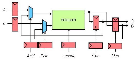
This project consists of the design and layout of a chip which contains a
datapath for a simple 8-bit processor that performs five basic operations,
has two enable-able output registers, and two individually-controllable
input ports.
Chips include clock trees, power rings and grid, Vdd/Gnd/input/output
I/O pads with the output pad sufficient for driving a 10 pF load.
Students produced all layout themselves.
The chips were laid out using TSMC's 0.18 μm CMOS and scalable
design rules.
"Top" is the highest-level test environment
that includes the complete chip and 10 pF loads on all outputs.
|
- Block diagram (chip)
- Block diagram (top)
|
Class: Area × Minimum Cycle Time (Delay)
|
|
| |
Min: |
8,252 μm2⋅ns
|
| |
Max: |
1,547,944 μm2⋅ns
|
| |
Median: |
61,377 μm2⋅ns
|
| |
Ratio max/min: |
188! |
|
Class: core.mag Area
|
|
| |
Min: |
10,839 μm2 |
| |
Max: |
93,374 μm2
|
| |
Median: |
19,191 μm2
|
| |
Ratio max/min: |
8.6 |
|
Class: top.mag Minimum Cycle Time (Delay)
|
|
| |
Min: |
0.43 ns |
| |
Max: |
27.2 ns |
| |
Median: |
3.26 ns |
| |
Ratio max/min: |
63! |
|
|
First place winners
|
| |
Chip core (shown to scale with 2nd place) |
Entire chip |
Ryan Godfrey
Michael Plumb
Area × Delay
= 8,252 μm2⋅ns
Core Area
= 19,191 μm2
Top-level Min Cycle Time = 0.43 ns
(2.33 GHz)
|
![[core]](19/godfrey-plumb-core.300wide.png)
|
![[chip]](19/godfrey-plumb-chip.250high.png)
|
|
Second place winners
|
| |
Chip core (shown to scale with 1st place) |
Entire chip |
Ziyuan Dong
Haotian Wu
Area × Delay
= 8,865 μm2⋅ns
Core Area = 17,048 μm2
Top-level Min Cycle Time = 0.52 ns
(1.92 GHz)
|
![[core]](19/dong-wu-core.213wide.png)
|
![[chip]](19/dong-wu-chip.250high.png)
|
| |
|
Fall 2018
|
|
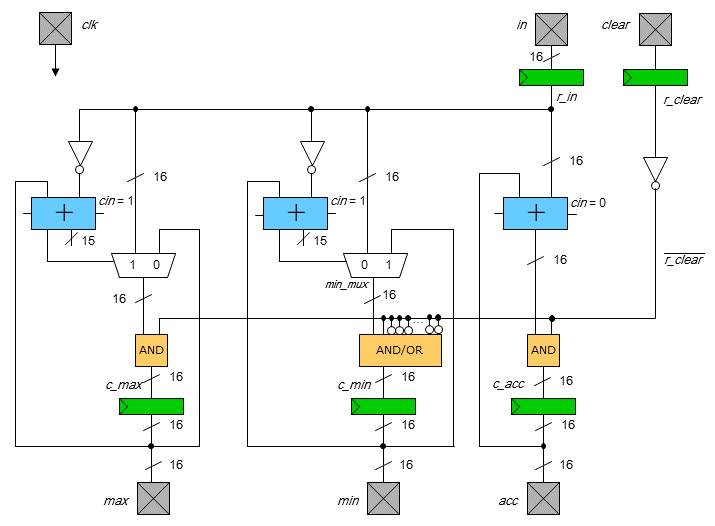
Project:
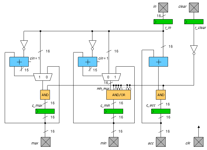
This project consists of the design and layout of a chip which accumulates
and finds the minimum and maximum of a series of input numbers.
All adders have 16-bit inputs and a 16-bit output.
The "AND" and "AND/OR" blocks contain 16 2-input gates with one input of all
gates connected to r_clear.
The two "AND" blocks contain 16 AND gates.
The "AND/OR" block contains 1 AND gate connected to the MSB of "min_mux"
and 15 OR gates with one input inverted tied to
r_clear
(i.e., out = in1 OR
in2).
The output
max is the maximum,
min is the minimum, and
acc is the accumulated sum
of all inputs since the last time clear was asserted.
Chips include clock trees, power rings and grid, Vdd/Gnd/input/output
I/O pads with the output pad sufficient for driving a 10 pF load.
Students produced all layout themselves.
The chips were laid out using TSMC's 0.18 μm CMOS and scalable
design rules.
"Top" is the highest-level test environment
that includes the complete chip and 10 pF loads on all outputs.
|
- Block diagram (chip)
- Block diagram (top)
|
Class: Area × Minimum Cycle Time (Delay)
|
|
| |
Min: |
23,593 μm2⋅ns
|
| |
Max: |
14,378,668 μm2⋅ns
|
| |
Median: |
309,105 μm2⋅ns
|
| |
Ratio max/min: |
610! |
|
Class: core.mag Area
|
|
| |
Min: |
10,822 μm2 |
| |
Max: |
686,883 μm2
|
| |
Median: |
38,161 μm2
|
| |
Ratio max/min: |
64! |
|
Class: top.mag Minimum Cycle Time (Delay)
|
|
| |
Min: |
1.60 ns |
| |
Max: |
210.4 ns |
| |
Median: |
8.10 ns |
| |
Ratio max/min: |
132! |
|
|
First place winners
|
| |
Chip core (shown to scale with 2nd place) |
Entire chip |
Andrea Hsieh
Zhouhao Yu
Area × Delay
= 23,593 μm2⋅ns
Core Area
= 14,745 μm2
Top-level Min Cycle Time = 1.60 ns
(625 MHz)
|
![[core]](18/hsieh-yu-core.300wide.png)
|
![[chip]](18/hsieh-yu-chip.250high.png)
|
|
Second place winners
|
| |
Chip core (shown to scale with 1st place) |
Entire chip |
Evan Sousa
Wesly Tonks
Area × Delay
= 27,991 μm2⋅ns
Core Area = 13,721 μm2
Top-level Min Cycle Time = 2.04 ns
(490 MHz)
|
![[core]](18/sousa-tonks-core.289WIDE.png)
|
![[chip]](18/sousa-tonks-chip.250high.png)
|
| |
|
Fall 2017
|
|
Project:
This project consists of the design and layout of a chip which
implements a simplified component of a
Display Stream Compression (DSC)
encoder. DSC is a state of the art video and image compression standard
that produces visually lossless quality images while requiring very small
chip area.
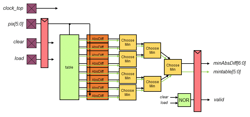
The project's DSC component is the Indexed Color History (ICH) block
which finds the best match between input pixels and pixels in a table,
all in one clock cycle.
Chips include clock trees, power rings and grid, Vdd/Gnd/input/output
I/O pads with the output pad sufficient for driving a 10 pF load.
Students produced all layout themselves.
The chips were laid out using TSMC's 0.18 μm CMOS and scalable
design rules.
"Top" is the highest-level test environment
that includes the complete chip and 10 pF loads on all outputs.
|
- Block diagram (chip)
- Block diagram (top)
|
Class: Area × Minimum Cycle Time (Delay)
|
|
| |
Min: |
46,638 μm2⋅ns
|
| |
Max: |
22,681,170 μm2⋅ns
|
| |
Median: |
261,913 μm2⋅ns
|
| |
Ratio max/min: |
486! |
|
Class: core.mag Area
|
|
| |
Min: |
18,631 μm2 |
| |
Max: |
1,008,052 μm2
|
| |
Median: |
66,409 μm2
|
| |
Ratio max/min: |
54! |
|
Class: top.mag Minimum Cycle Time (Delay)
|
|
| |
Min: |
0.88 ns |
| |
Max: |
49.6 ns |
| |
Median: |
6.70 ns |
| |
Ratio max/min: |
7.6 |
|
|
First place winners
|
| |
Chip core (shown to scale with 2nd place) |
Entire chip |
Tracy He
Yuhua Wu
Area × Delay = 46,638 μm2⋅ns
Core Area = 52,998 μm2
Top Min Cycle Time = 0.88 ns
(1.14 GHz)
|
![[core]](17/he-wu-core.232wide.png)
|
![[chip]](17/he-wu-chip.250high.png)
|
|
Second place winners
|
| |
Chip core (shown to scale with 1st place) |
Entire chip |
Arthur Hlaing
Delvin Huynh
Area × Delay = 52,539 μm2⋅ns
Core Area = 18,631 μm2
Top Min Cycle Time = 2.82 ns
(355 MHz)
|
![[core]](17/hlaing-huynh-core.300wide.png)
|
![[chip]](17/hlaing-huynh-chip.250high.png)
|
| |
|
Fall 2016
|
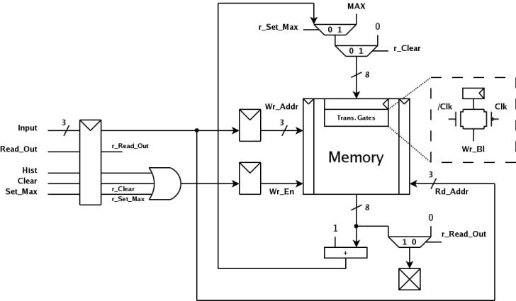
- Project:
-
This project consists of the design, floorplanning,
and full-custom layout of a chip which generates a
histogram of a series
of unsigned input numbers utilizing eight "bins" or "intervals".
The chip contains an 8-word × 8-bit memory built with 64 discrete
flip-flops, an 8-bit ripple-carry adder, and other logic blocks.
All memory elements are clocked on the positive clock edges.
The chip has 3 primary modes:
        Mode              clear   calc_hist  read_out     input[2:0]
   -------------------    -----     -----      -----     ---------------
   Clear memory             1         0          0       Address values 0-7
   Calculate histogram      0         1          0       3-bit data value
   Read out memory          0         0          1       Address values 0-7
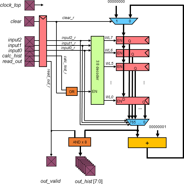
Chips include clock trees, power rings
and grid, Vdd/Gnd/input/output
I/O pads with the output pad sufficient for driving a 10 pF load.
Students produced all layout themselves.
The chips were laid out using TSMC's 0.18 μm CMOS and scalable
design rules.
"Top" is the highest-level test environment
that includes the complete chip and 10 pF loads on all outputs.
- Block diagram (chip)
- Block diagram (top)
- Overall class area × delay
|
|
First place winners
|
| |
Chip core (shown to scale with 2nd place) |
Entire chip |
Sarvagya Singh
Swathi Sundar
Area × Delay = 3862 μm2⋅ns
Core Area = 8217 μm2
Top Delay = 0.47 ns
(2.1 GHz)
|
![[core]](16/singh-sundar-core.300wide.png)
|
![[chip]](16/singh-sundar-chip.250high.png)
|
|
Second place winners
|
| |
Chip core (shown to scale with 1st place) |
Entire chip |
Kirtanpal Ghoman
Vidush Vishwanath
Area × Delay = 4485 μm2⋅ns
Core Area = 8306 μm2
Top Delay = 0.54 ns
(1.9 GHz)
|
![[core]](16/ghoman-vishwanath-core.239wide.png)
|
![[chip]](16/ghoman-vishwanath-chip.250high.png)
|
| |
|
Fall 2015
|
- Project:
-
This project consists of the design and layout of a chip which implements a
hardware-based 4-bit unsigned parallel sorting chip. There are 4 separate
unsigned 4-bit inputs of unsorted numbers. Each of these unsorted number
streams are sorted by a stream of 4 processing elements, that each individually
perform a 5-value bubble sort. Finally, each of these 4 sorted lists will
be merged by 3 merge-processing elements. The chip sorts so that the highest
value is output first and the lowest input value is output last.
To assure a valid sorted list, after up to 5 sets of valid input data, all of
the data input and data valid must be set to 0 for at least 16 clock cycles
to flush the sorted data out.
 Chips include clock trees, power rings
and grid, Vdd/Gnd/input/output
I/O pads with the output pad sufficient for driving a 10 pF load.
Students produced all layout themselves.
The chips were laid out using TSMC's 0.18 μm CMOS and scalable
design rules.
Chips include clock trees, power rings
and grid, Vdd/Gnd/input/output
I/O pads with the output pad sufficient for driving a 10 pF load.
Students produced all layout themselves.
The chips were laid out using TSMC's 0.18 μm CMOS and scalable
design rules.
- Block diagram (chip)
- Block diagram (top)
- Overall class area x delay
|
|
First place winners
|
| |
Chip core (shown to scale with 2nd place) |
Entire chip |
Mark Hildebrand
Shifu Wu
Core Area x Delay = 53 μm2⋅ns
Core Area = 379 μm2
Core Delay = 0.14 ns
(6.2 GHz!)
|
![[core]](15/hildebrand-wu-core.115wide.png)
|
![[chip]](15/hildebrand-wu-chip.250high.png)
|
|
Second place winners
|
| |
Chip core (shown to scale with 1st place) |
Entire chip |
Yanpeng Dong
Yugang Jing
Core Area x Delay = 968 μm2⋅ns
Core Area = 871 μm2
Core Delay = 0.90 ns
|
![[core]](15/dong-jing-core.300wide.png)
|
![[chip]](15/dong-jing-chip.250high.png)
|
| |
|
Fall 2014
|
- Project:
-
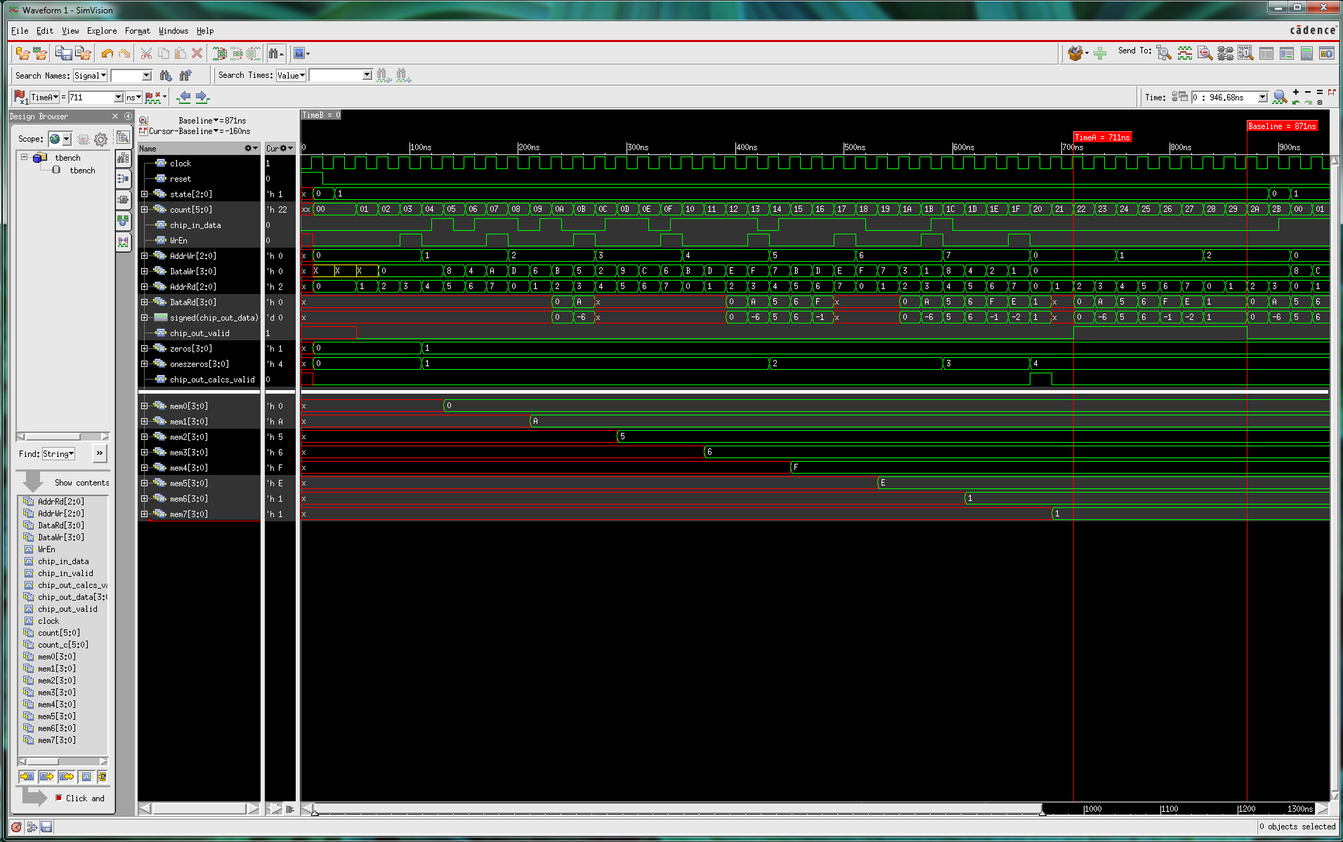
This project consists of the design and layout of a chip which inputs
a serial stream of 32 bits and outputs the bits in the form of 8
4-bit words.
So the design can be scalable to handle very large bit streams, the
internal memory is built with an SRAM memory array—which has 8
words of 4-bits each in this design.
Although the chip functions on a continuous 32-bit stream of bits, we can
also think of the 32-bits as being eight 4-bits 2's complement numbers.
The first four bits to enter the chip are output as the first 4-bit word,
the next four bits as the second 4-bit word, etc.
Within each 4-bit group however, you may consider that the
first bit to enter the chip is the LSB (as shown in the waveforms), or the MSB--both are fine.
In a similar manner to a critical core function of a CAVLC entropy coder* in
the H.264 video compression standard, your chip must count the number of
4-bit words values that are (+1, 0, -1) and output the
4-bit value as oneszeros. It must also calculate and output
zeros which is the number of 4-bit values equal to zero.
* The H.264
video compression standard is widely used in advanced
video applications such as Blu-ray and YouTube. The CAVLC
encoder in H.264 contains a step where the number of values at the end of
a string of numbers that are either (+1, 0, -1) must be counted.
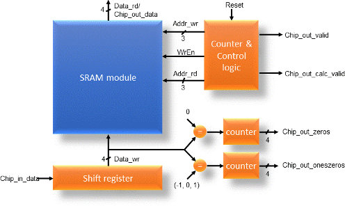 Chips include clock trees, power rings
and grid, Vdd/Gnd/input/output
I/O pads with the output pad sufficient for driving a 10 pF load.
Students produced all layout themselves.
The chips were laid out using TSMC's 0.18 μm CMOS and scalable
design rules.
Chips include clock trees, power rings
and grid, Vdd/Gnd/input/output
I/O pads with the output pad sufficient for driving a 10 pF load.
Students produced all layout themselves.
The chips were laid out using TSMC's 0.18 μm CMOS and scalable
design rules.
- Block diagram (chip)
- Block diagram (top)
- Overall class area x delay
|
|
First place winners
|
| |
Chip core (shown to scale with 2nd place) |
Entire chip |
Eduard Alfonso
Andrew Chung
Core Area x Delay = 363,501 μm2⋅ns
Core Area = 1,346,301 μm2
Core Delay = 0.27 ns
(3.7 GHz!)
|
![[core]](14/alfonso-chung-core.144wide.jpg)
|
![[chip]](14/alfonso-chung-chip.325high.jpg)
|
|
Second place winners
|
| |
Chip core (shown to scale with 1st place) |
Entire chip |
Chris Bonham
Jeremy Watkins
Core Area x Delay = 5,391,550 μm2⋅ns
Core Area = 3,098,592 μm2
Core Delay = 1.74 ns
|
![[core]](14/bonham-watkins-core.325wide.jpg)
|
![[chip]](14/bonham-watkins-chip.325high.jpg)
|
| |
|
Fall 2013
|
- Project:
-
This project consists of the design and layout of a chip which contains
an array of 9 processors that sorts a stream of 9 unsigned 8-bit numbers
at very high throughputs. The chip uses a novel algorithm that can
be viewed as a scalable physically-distributed multi-processor bubble sort where
data flows once through 9 2-element sorting processors rather than one
processor making ~9 passes through the data set as would happen in a
common software implementation. If a single-issue RISC processor required
7 cycles to perform a single comparison and swap (load, load, subtract,
branch, store, store, incr_counter), to maintain the same performance
as a 2.0 GHz array of these processors, the RISC processor would
need to run at 126 GHz!
A diagram of the key circuits in each processor and the 3x3 array of
processors in core.mag is shown below:
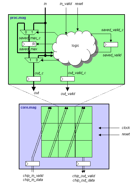 Chips include clock trees, power rings
and grid, Vdd/Gnd/input/output
I/O pads with the output pad sufficient for driving a 10 pF load.
Students produced all layout themselves.
The chips were laid out using TSMC's 0.18 μm CMOS and scalable
design rules.
Chips include clock trees, power rings
and grid, Vdd/Gnd/input/output
I/O pads with the output pad sufficient for driving a 10 pF load.
Students produced all layout themselves.
The chips were laid out using TSMC's 0.18 μm CMOS and scalable
design rules.
- Block diagram (chip)
- Block diagram (top)
- Overall class area x delay
|
|
First place winners
|
| |
Chip core (shown to scale with 2nd place) |
Entire chip |
Kenneth Broce
Huan Zhang
Core Area x Delay = 2,764,566 μm2⋅ns
Core Area = 2,559,783 μm2
Core Delay = 1.08 ns
|
![[core]](13/broce-zhang-core.to-scale.jpg)
|
![[chip]](13/broce-zhang-top.325high.jpg)
|
|
Second place winners
|
| |
Chip core (shown to scale with 1st place) |
Entire chip |
Timothy Andreas
Tam Quach
Core Area x Delay = 3,461,370 μm2⋅ns
Core Area = 6,922,740 μm2
Core Delay = 0.50 ns
|
![[core]](13/andreas-quach-core.325high.jpg)
|
![[chip]](13/andreas-quach-top.325high.jpg)
|
| |
|
Fall 2012
|
- Project:
-
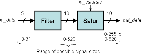
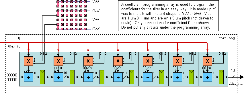
This project requires the design and layout of a chip which contains
a high-speed digital low-pass filter. Filters are one of the most common
blocks found in digital signal processors, which are increasingly popular
in many electronic systems.
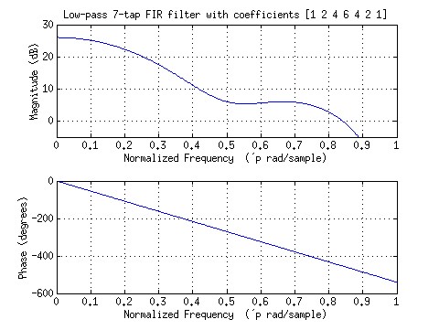
The filter is a 5-tap or 5-coefficient finite impulse response (FIR)
filter and has a saturator at its output. It processes one
sample every clock cycle enabling very high data throghputs. The plot
below shows the magnitude frequency response of an example 7-tap filter
(with a phase plot below it). The values of the coefficients determine
the specifications and type of the filter (e.g. low-pass, high-pass, etc.).
 The filter consists of three major components: 1) multipliers, 2) adders, and
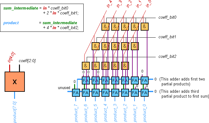
3) registers made up of flip-flops. Use the multiplier from your Hwk as a
starting point and revise it at least once to improve its area and speed.
The filter consists of three major components: 1) multipliers, 2) adders, and
3) registers made up of flip-flops. Use the multiplier from your Hwk as a
starting point and revise it at least once to improve its area and speed.
The adders must be built with a simple ripple-carry adder structure made up of
a chain of full adders.
The multipliers must be built using the structure shown in Figure 11-30
in the textbook. You may use Full Adders or Half Adders for the "HA"
blocks.
The filter is followed by a saturator which saturates or clips the output
to be no greater than a certain level.
Saturation is a common method to reduce the magnitude and word-width of
signals and in some sense is complimentary to
rounding.
The 5 coefficients of the filter and the saturation level are programmable.

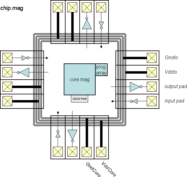
Chips include clock trees, power rings
and grid, Vdd/Gnd/input/output
I/O pads with the output pad sufficient for driving a 10 pF load.
Students produced all layout themselves.
The chips were laid out using TSMC's 0.18 μm CMOS and scalable
design rules.
- Block diagram (chip)
- Block diagram (top)
- Overall class area x delay
|
|
First place winners
|
| |
Chip core (shown to scale with 2nd place) |
Entire chip |
Busheng Lou
Vrushti Modi
Design is fully correct
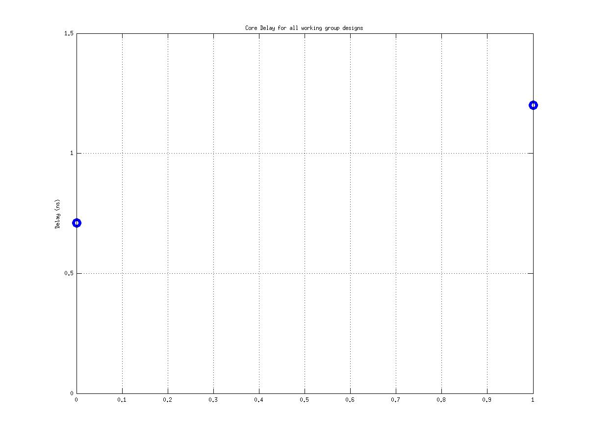
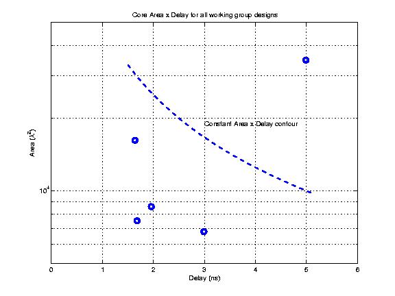
Core Area x Delay = 335,850 μm2⋅ns
Core Area = 128,678 μm2
Core Delay = 2.61 ns
|
![[core]](12/lou.core.325high.jpg)
|
![[chip]](12/lou.chip.325high.jpg)
|
|
Second place winners
|
| |
Chip core (shown to scale with 1st place) |
Entire chip |
Binbin Fu
Cuichenzhi Huang
Superb design however output has minor bit errors in test sequence two
Core Area x Delay = 40,137 μm2⋅ns
Core Area = 81,913 μm2
Core Delay = 0.49 ns
|
![[core]](12/fu.core.to-scale.jpg)
|
![[chip]](12/fu.chip.325high.jpg)
|
| |
|
Fall 2010
|
- Project:
- This project requires the design and layout of a datapath for
a simple 8-bit processor that performs five basic operations, has
two enable-able output registers, and two individually-controllable
input ports.
The datapath performs the following operations:
1) bitwise AND,
2) bitwise OR,
3) bitwise XOR,
4) Add. (only the least-significant 8 bits), and
5) Multiply. (only the least-significant 8 bits).
Chips include clock trees, power rings
and grid, Vdd/Gnd/input/output
I/O pads with the output pad sufficient for driving a 10 pF load.
Students produced all layout themselves.
The chips were laid out using TSMC's 0.18 μm CMOS and scalable
design rules.
- Block diagram (chip)
- Block diagram (top)
- Overall class area x delay
- Overall class chip-core area
- Min: 17,036 μm2
- Max: 682,683 μm2
- Median: 52,622 μm2
- Ratio max/min: 40.1!
- Overall class delay
- Min: 0.95 ns
- Max: 12,490 ns
- Median: 28.40 ns
- Ratio max/min: 13,147!
|
|
First place winners
|
| |
Chip core |
Entire chip |
Sean Burkhardt-Corcoran
Mohammad Amin Heydari
Core Area x Delay = 16,116 μm2⋅ns
Core Area = 17,036 μm2
Core Delay = 0.95 ns
|
![[core]](10b.fall/sb.ah-core.300wide.jpg)
|
![[chip]](10b.fall/sb.ah-chip.325pixels.jpg)
|
|
Second place winners
|
| |
Chip core |
Entire chip |
Val Apgar
Matthew Spriggs
Core Area x Delay = 242,062 μm2⋅ns
Core Area = 52,622 μm2
Core Delay = 4.60 ns
|
![[core]](10b.fall/va.ms-core.400wide.jpg)
|
![[chip]](10b.fall/va.ms-chip.325pixels.jpg)
|
| |
|
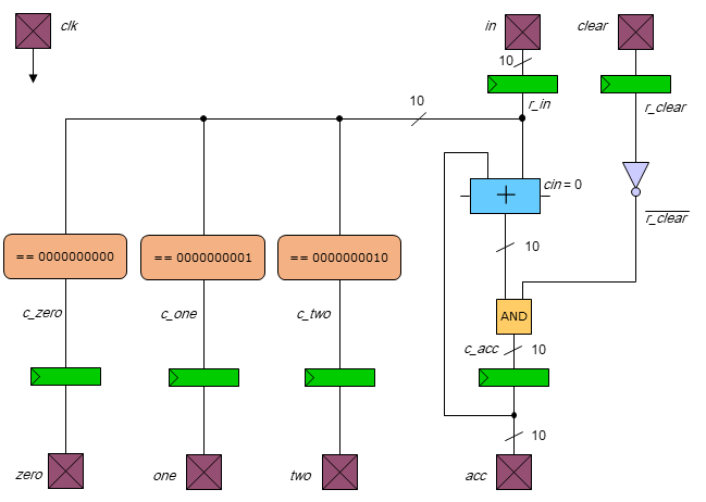
Winter 2010
|
- Project:
- The purpose of this project is to lay out the major portions
of a simple digital chip that accumulates and finds the maximum
and minimum of a series of input numbers.
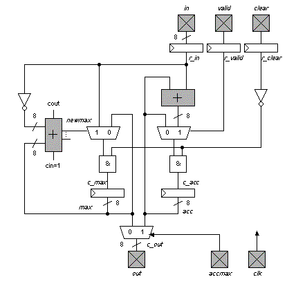
The circuits of the chip are shown below.
The inputs are: a 16-bit in, and single bit
clear, and clk.
The outputs are 16-bit max, min, and acc.
Operation of the chip begins by setting clear=1 for at least
one cycle to clear all three outputs.
The output acc is the accumulated sum,
max is the current maximum, and
min is the current minimum of all inputs since the last clearing
operation.
Chips include clock trees, power rings
and grid, Vdd/Gnd/input/output
I/O pads with the output pad sufficient for driving a 10 pF load.
Students produced all layout themselves.
The chips were laid out using TSMC's 0.18 μm CMOS and scalable
design rules.
- Block diagram (chip)
- Block diagram (top)
- Overall class area x delay
- :Overall class area
- Min: 43,500 μm2
- Max: 334,000 μm2
- Ratio max/min: 7.7
- :Overall class delay
- Min: 2.20 ns
- Max: 50.0 ns
- Ratio max/min: 22.7
|
|
First place winners
|
| |
Chip core |
Entire chip |
Brian Zimmer
Ritesh Patel
Core Area x Delay = 201,695 μm2⋅ns
Core Area = 25,275 μm2
Core Delay = 7.92 ns
|
![[core]](10a.wtr/bz.rp-core.325wide.jpg)
|
![[chip]](10a.wtr/bz.rp-chip.325high.jpg)
|
|
Second place winners
|
| |
Chip core |
Entire chip |
David Tu
Ivan Charcos
Core Area x Delay = 229,115 μm2⋅ns
Core Area = 37,933 μm2
Core Delay = 6.04 ns
|
![[core]](10a.wtr/dt.ic-core.325wide.jpg)
|
![[chip]](10a.wtr/dt.ic-chip.325high.jpg)
|
|
Honorable Mention for Minimum Area
|
| |
Chip core |
|
Keith MacMillan
Srivigyan Chandu
Core Area = 20,434 μm2
|
![[core]](10a.wtr/honorable.core.200wide.jpg)
|
| |
|
2009
|
- Project:
- The purpose of this project is to design and layout a chip
which contains a high-speed programmable digital filter. Filters are
one of the most common blocks found in digital signal processing
systems, which are increasingly popular in many electronic systems.
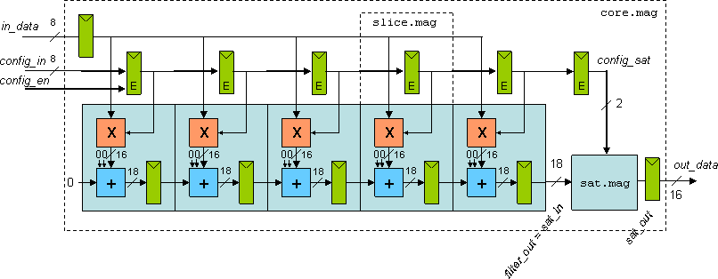
The filter is a 5-tap or 5-coefficient finite impulse response (FIR)
filter with a saturator at its output. It processes one input sample
and produces one output sample every clock cycle enabling very high
data throughputs. The values of the coefficients determine the
specifications and type of the filter (e.g. low-pass, high-pass,
etc.) and are programmable. The filter is composed of five
identical slices which each consist of three major components: 1)
a multiplier, 2) an adder, and 3) registers made up of flip-flops.
The slices are designed such that much longer filters can be
implemented with the exact same layout by only increasing the
number of slices.
Chips include clock trees, power rings and power grid,
Vdd/Gnd/input/output I/O pads with the output pad sufficient for
driving a 10 pF load.
Students produced all layout themselves.
The chips were laid out using TSMC's 0.18 μm CMOS and scalable
design rules.
The two core chip plots below are shown to scale with respect to each
other.
- Block diagram (chip)
- Block diagram (top)
- Overall class area x delay
- Overall class area:
- Min: 43,500 μm2
- Max: 334,000 μm2
- Ratio max/min: 7.7
- Overall class delay:
- Min: 2.20 ns
- Max: 50.0 ns
- Ratio max/min: 22.7
|
|
First place winners
|
| |
Chip core |
Entire chip |
Quyen Phung
Yuan Hui Li
Core Area x Delay = 152,900 μm2⋅ns
Core Area = 69,500 μm2
Core Delay = 2.20 ns
|
![[core]](09/qp.yl-core.264x450.jpeg)
|
![[chip]](09/qp.yl-chip.325pixels.jpeg)
|
|
Second place winners
|
| |
Chip core |
Entire chip |
Gary Chung
Jon Pimentel
Core Area x Delay = 165,735 μm2⋅ns
Core Area = 43,500 μm2
Core Delay = 3.81 ns
|
![[core]](09/gc.jp-core.267x278.jpeg)
|
![[chip]](09/gc.jp-chip.325pixels.jpeg)
|
| |
|
2008
|
- Project:
- The purpose of this project is to design and layout a chip
which contains a high-speed digital low-pass filter. Filters are
one of the most common blocks found in digital signal processors,
which are increasingly popular in many electronic systems.
The filter is a 7-tap finite impulse response (FIR) filter and
has a saturator at its output. It processes one complete sample
every clock cycle enabling very high data throghputs.
The filter consists of three components: 1) multipliers, 2) adders,
and 3) registers made up of flip-flops.
The purpose of the saturator is to clamp or saturate the filter's
output from a maximum of 620 to a maximum of 255--so it fits into
an 8-bit word.
The filter is highly pipelined into 7 pipeline stages.
Chips include clock trees, power rings
and grid, Vdd/Gnd/input/output
I/O pads with the output pad sufficient for driving a 10 pF load.
Students produced all layout themselves.
The chips were laid out using TSMC's 0.18 μm CMOS and scalable
design rules.
- Datapath block diagrams:
Filter and saturator,
filter,
multiplier.
- Block diagram (chip)
- Block diagram (top)
- Overall class area x delay
- Overall class area:
- Min: 2,409,940 λ2
- Max: 4,079,496 λ2
- Ratio max/min: 1.7
- Overall class delay:
- Min: 0.34 ns
- Max: 0.51 ns
- Ratio max/min: 1.5
|
|
First place winners
|
| |
Chip core |
Entire chip |
Greg Fattig
Allen Tang
Core Area x Delay = 819,379 λ2⋅ns
Core Area = 2,409,940 λ2
= 19,520 μm2
Core Delay = 0.34 ns
|
![[core]](08/gf.at-core.450pixels.jpg)
|
![[chip]](08/gf.at-chip.325pixels.jpg)
|
|
Second place winners
|
| |
Chip core |
Entire chip |
Ba Duong
Yifan Liu
Core Area x Delay = 2,080,542 λ2⋅ns
Core Area = 4,079,496 λ2
= 33,044 μm2
Core Delay = 0.51 ns
|
![[core]](08/bd.yl-core.450pixels.jpg)
|
![[chip]](08/bd.yl-chip.325pixels.jpg)
|
| |
|
2007
|
- Project:
-
In this project, students design and layout a chip which contains
an array of 100 processors that sorts a stream of 100 unsigned
8-bit numbers at very high speed. The chip uses a type of bubble
sorting algorithm where data flows through 100 2-element sorting
processors (rather than one processor making 100 passes through the
data set as would happen in a common software implementation). If a
single-issue RISC processor requires 7 cycles to perform a single
comparison and swap (load, load, subtract, branch, store, store,
incr_counter), to maintain the same performance as a 1.0 GHz array
of processors, the RISC processor would have to run at 700 GHz!
Each processor is pipelined and includes reset and data valid
input and output signals. Chips include clock trees, power rings
and grid, Vdd/Gnd/input/output
I/O pads with the output pad sufficient for driving a 10 pF load.
Students produced all layout themselves.
The chips were laid out using TSMC's 0.18 μm CMOS and scalable
design rules.
- Block diagram (processor and core)
- Block diagram (chip)
- Block diagram (top)
- Overall class area x delay
- Overall class area: (one processor)
- Min: 379,735 λ2
- Max: 4,427,821 λ2
- Median: 445,176 λ2
- Ratio max/min: 11.7
- Overall class delay:
- Min: 0.71 ns
- Max: 10.00 ns
- Median: 1.25 ns
- Ratio max/min: 14.1
|
|
First place winners
|
| |
Chip core |
Entire chip |
Anh Tran
Ning Xu
Core Area x Delay = 35,394,551 λ2⋅ns
Core Area = 49,851,481 λ2
Core Delay = 0.71 ns
|
![[core]](07/at.nx-core.sm.jpg)
|
![[chip]](07/at.nx-chip.325pixels.jpg)
|
|
Second place winners
|
| |
Chip core |
Entire chip |
Khadar Shaik
Eian Vizzini
Core Area x Delay = 63,670,687 λ2⋅ns
Core Area = 50,936,550 λ2
Core Delay = 1.25 ns
|
![[core]](07/ks.ev-core.sm.jpg)
|
![[chip]](07/ks.ev-chip.325pixels.jpg)
|
|
2006
|
- Project:
- Full-custom histogram calculator chip which computes an 8-point
histogram on an arbitrary stream of inputs with up to 255 inputs
per histogram "bin".
The datapath is pipelined and includes reset and read out modes,
and special circuits to aid in measuring the processor's critical
path.
Chips include clock trees, power rings and grid, Vdd/Gnd/input/output
I/O pads with the output pad sufficient for driving a 10 pF load.
Students produced all layout themselves.
The chips were laid out using TSMC's 0.18 μm CMOS and scalable
design rules with λ = 0.09μm.
- Block diagram (processor)
- Block diagram (chip-level)
- Overall class area x delay
- Overall class area:
- Min: 836,300 λ2
- Max: 4,300,000 λ2
- Median: 1,675,300 λ2
- Ratio max/min: 5.1
- Overall class delay:
- Min: 1.64 ns
- Max: 4.99 ns
- Median: 1.96 ns
- Ratio max/min: 3.1
|
|
First place winners
|
| |
Chip core |
Entire chip |
Neil Jacklin
Kyle Piper
Core Area x Delay = 1,558,700 λ2⋅ns
Core Area = 927,800 λ2
Core Delay = 1.68 ns
|
![[core]](06/nj.kp-core.sm.jpg)
|
![[chip]](06/nj.kp-chip.sm.jpg)
|
|
Second place winners
|
| |
Chip core |
Entire chip |
Brent Bohnenstiehl
Maggie Zhang
Core Area x Delay = 2,081,700 λ2⋅ns
Core Area = 1,062,100 λ2
Core Delay = 1.96 ns
|
![[core]](06/mz.bb-core.sm.jpg)
|
![[chip]](06/mz.bb-chip.sm.jpg)
|
|
Honorable mention (smallest area)
|
| |
Chip core |
Entire chip |
Sam Lee
Jia Ming Mar
Core Area x Delay = 2,500,500 λ2⋅ns
Core Area = 836,300 λ2
Core Delay = 2.99 ns
|
![[core]](06/sl.jm-core.sm.jpg)
|
![[chip]](06/sl.jm-chip.sm.jpg)
|
|
2005
|
- Project:
- Full-custom chip which calculates the accumulated sum,
maximum input, and minimum input of a stream of 8-bit input data.
The datapath is pipelined and includes reset circuits for all three
outputs.
Chips include clock trees, power rings and grid, Vdd/Gnd/input/output
I/O pads with the output pad sufficient for driving a 10 pF load.
Students produced all layout themselves.
The chips were laid out using TSMC's 0.18 μm CMOS and scalable
design rules with λ = 0.09μm.
- Overall class area x delay
- Overall class area:
- Min: 545,600 λ2
- Max: 3,182,652 λ2
- Median: 840,984 λ2
- Ratio max/min: 5.8
- Overall class delay:
- Min: 0.39 ns
- Max: 5.00 ns
- Median: 1.31 ns
- Ratio max/min: 12.8
|
|
First place winners
|
| |
Chip core |
Entire chip |
Chi Chen
Tyrone Tracy
Core Area x Delay = 212,784 λ2⋅ns
Core Area = 545,600 λ2
Core Delay = 0.39 ns
|
![[core]](05/cc.tt.core-sm.jpg)
|
![[chip]](05/cc.tt.chip-sm.jpg)
|
|
Second place winners
|
| |
Chip core |
Entire chip |
Brian Swenson
Matthew Kong
Core Area x Delay = 323,084 λ2⋅ns
Core Area = 547,600 λ2
Core Delay = 0.59 ns
|
![[core]](05/bs.mk.core-sm.jpg)
|
![[chip]](05/bs.mk.chip-sm.jpg)
|
| |
| |
|
2004
|
- Project:
- Layout for a full-custom digital processing chip that accumulates
and finds the maximum of a series of input numbers.
The processor has three primary inputs:
an 8-bit data word, a valid signal, and a clear signal.
The circuit has a switchable output that shows one of two values:
1) the accumulation of all inputs since the last clear, and
2) the maximum value since that last clear.
The datapath is pipelined and includes necessary reset circuits.
Chips include clock trees, power rings and grid, Vdd/Gnd/input/output
I/O pads with the output pad sufficient for driving a 10 pF load.
Students produced all layout themselves.
The chips were laid out using TSMC's 0.18 μm CMOS and scalable
design rules with λ = 0.09μm.
- Overall class area
- Min: 638,448 λ2
- Max: 9,037,825 λ2
- Ratio max/min: 14.2
- Overall class delay
- Min: 5.38 ns
- Max: 40.0 ns
- Ratio max/min: 7.4
|
|
First place winners
|
| |
|
|
Andy Swing
Steven Tin
Core Area x Delay = 5,209,736 λ2⋅ns
Core Area = 638,448 λ2
Core Delay = 8.16 ns
|
|
|
|
Second place winners
|
| |
|
|
Andrew Luo
Sofia Hao
Core Area x Delay = 6,193,937 λ2⋅ns
Core Area = 891,214 λ2
Core Delay = 6.95 ns
|
|
|
![[Kemper Hall second floor VLSI Hall of Fame case]](hall.case.2013.jpg)
![[core]](23/ricci-core.423wide.png)
![[chip]](23/ricci-chip.500wide.png)
![[core]](23/wang-core.600wide.png)
![[chip]](23/wang-chip.500wide.png)
![[core]](21/arbuckle-core.500wide.png)
![[chip]](21/arbuckle-chip.500wide.png)
![[core]](21/abbott-core.400wide.png)
![[chip]](21/abbott-chip.500wide.png)
![[core]](20/sun-core.489wide.png)
![[chip]](20/sun-chip.468wide.png)
![[core]](20/mao-core.488wide.png)
![[chip]](20/mao-chip.425wide.png)
![[core]](19/godfrey-plumb-core.500wide.png)
![[chip]](19/godfrey-plumb-chip.500high.png)
![[core]](19/dong-wu-core.355wide.png)
![[chip]](19/dong-wu-chip.500high.png)
![[core]](18/hsieh-yu-core.500wide.png)
![[chip]](18/hsieh-yu-chip.500high.png)
![[core]](18/sousa-tonks-core.500wide.png)
![[chip]](18/sousa-tonks-chip.500high.png)
![[core]](17/he-wu-core.600wide.png)
![[chip]](17/he-wu-chip.500high.png)
![[core]](17/hlaing-huynh-core.600wide.png)
![[chip]](17/hlaing-huynh-chip.500high.png)
![[core]](16/singh-sundar-core.600wide.png)
![[chip]](16/singh-sundar-chip.500high.png)
![[core]](16/ghoman-vishwanath-core.479wide.png)
![[chip]](16/ghoman-vishwanath-chip.500high.png)
![[core]](15/hildebrand-wu-core.600wide.png)
![[chip]](15/hildebrand-wu-chip.500high.png)
![[core]](15/dong-jing-core.600wide.png)
![[chip]](15/dong-jing-chip.500high.png)
![[core]](14/alfonso-chung-core.288wide.jpg)
![[chip]](14/alfonso-chung-chip.png)
![[core]](14/bonham-watkins-core.650wide.jpg)
![[chip]](14/bonham-watkins-chip.png)
![[core]](13/broce-zhang-core.jpg)
![[chip]](13/broce-zhang-top.jpg)
![[core]](13/andreas-quach-core.jpg)
![[chip]](13/andreas-quach-top.jpg)
![[core]](12/lou.core.jpg)
![[chip]](12/lou.chip.jpg)
![[core]](12/fu.core.jpg)
![[chip]](12/fu.chip.jpg)
![[core]](10b.fall/sb.ah-core.800wide.jpg)
![[chip]](10b.fall/sb.ah-chip.jpg)
![[core]](10b.fall/va.ms-core.800wide.jpg)
![[chip]](10b.fall/va.ms-chip.jpg)
![[core]](10a.wtr/bz.rp-core.bmp)
![[chip]](10a.wtr/bz.rp-chip.800wide.jpg)
![[core]](10a.wtr/dt.ic-core.bmp)
![[chip]](10a.wtr/dt.ic-chip.800wide.jpg)
![[core]](10a.wtr/honorable.core.bmp)
![[core]](09/qp.yl-core.587x1000.jpeg)
![[chip]](09/qp.yl-chip.jpeg)
![[core]](09/gc.jp-core.962x1000.jpeg)
![[chip]](09/gc.jp-chip.jpeg)
![[core]](08/gf.at-core.jpg)
![[chip]](08/gf.at-chip.jpg)
![[core]](08/bd.yl-core.jpg)
![[chip]](08/bd.yl-chip.jpg)
![[core]](07/at.nx-core.jpg)
![[chip]](07/at.nx-chip.jpg)
![[core]](07/ks.ev-core.jpg)
![[chip]](07/ks.ev-chip.png)
![[core]](06/nj.kp-core.jpg)
![[chip]](06/nj.kp-chip.jpg)
![[core]](06/mz.bb-core.jpg)
![[chip]](06/mz.bb-chip.jpg)
![[core]](06/sl.jm-core.jpg)
![[chip]](06/sl.jm-chip.jpg)
![[core]](05/cc.tt.core.jpg)
![[chip]](05/cc.tt.chip.jpg)
![[core]](05/bs.mk.core.jpg)
![[chip]](05/bs.mk.chip.jpg)